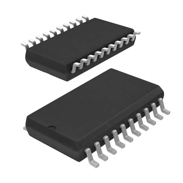
Renesas Electronics 74FCT3807SOG — Clock & Timing ICs

74FCT3807SOG Renesas 1:10 Fanout Buffer 100 MHz 20-SOIC

MPN74FCT3807SOG
End of Life

Renesas 74FCT3807SOG, 74FCT series, Fanout Buffer (Distribution), 1:10 ratio, LVTTL input, CMOS/TTL output, 100 MHz max, 3V to 3.6V supply, 0°C to 70°C, 20-SOIC surface mount package, tube.

$1.88Ref. price · indicative, final on quote
Packaging20-SOIC (0.295", 7.50mm Width)
StockContact for availability
MOQ1 pcs
  • 100% new & originalTraceable channels only — no refurbs, no pulls, no remarked parts.
  • Date & lot codes on quoteStated per line before you commit; label photos on request.
  • MSL-compliant ESD packingMoisture-sealed bags with indicator cards; reels photo-verified.
  • PayPal buyer protectionPay by T/T, PayPal or Payoneer — card payments covered end to end.

Specifications

74FCT3807SOG Technical Specifications
ParameterValue
TypeFanout Buffer (Distribution)
Series74FCT
Mounting typeSurface Mount
Voltage3V ~ 3.6V
Frequency100 MHz
Operating temperature0°C ~ 70°C
InputLVTTL
OutputCMOS, TTL
PackageTube
Case20-SOIC (0.295\", 7.50mm Width)
Number of circuits1
Ratio - Input:Output1:10
Differential - Input:OutputNo/No

Product details

What this 1:10 clock buffer does on your board

The 74FCT3807SOG is a single-circuit fanout buffer that takes one LVTTL clock input and distributes it to ten CMOS or TTL outputs. The 1:10 ratio means you can drive up to ten clock loads from one source without loading the upstream oscillator or PLL — the buffer isolates the input side from the output capacitance. Maximum frequency is 100 MHz.

Supply voltage and logic compatibility

The supply range is 3V to 3.6V. This is a 3.3V nominal part — it does not accept 5V on the input or output pins. If your upstream clock source is 5V LVCMOS, you need a level translator or a series resistor clamp before the 74FCT3807SOG input. The outputs are CMOS and TTL compatible at 3.3V, which matches most modern FPGAs, ASICs, and 3.3V microcontrollers. The input is LVTTL, which thresholds at 0.8V (VIL) and 2.0V (VIH) typical — that is a 1.2V noise margin at 3.3V. If your clock source swings rail-to-rail 3.3V, the input stage sees clean logic levels. A 1.8V or 2.5V clock source will not meet the VIH threshold without external biasing.

Active production and sourcing posture

Renesas continues to manufacture the 74FCT series, and this part is ROHS3 compliant. For BOM planning, this means no forced redesign for obsolescence in the near term.

What the 100 MHz and 1:10 ratio mean for your timing budget

At 100 MHz the period is 10 ns. The non-differential input and output (No/No) means this is a single-ended clock distribution part.

Frequently asked questions

Is 74FCT3807SOG compatible with 5V logic?

No. The supply range is 3V to 3.6V, and the input is LVTTL, which thresholds at 2.0V VIH. A 5V input signal exceeds the absolute maximum input voltage for the 3.3V process — use a level translator or a resistive divider before the input pin.