Clock fanout buffer — one input, ten outputs
The Renesas 74FCT3807QGI is a 1:10 fanout buffer that takes a single LVTTL clock input and distributes it to ten CMOS/TTL outputs. It is a non-inverting, non-differential buffer — no PLL, no jitter attenuation, no divide or multiply. What goes in at the input comes out at each output, just fanned out and re-driven. Maximum frequency is 100 MHz, which suits it for clock distribution in 74FCT, ALVC, or AVC logic systems, FPGA configuration clocks, and general-purpose synchronous bus trees. The supply range is 3V to 3.6V, so it runs cleanly off a 3.3V rail without an extra regulator.
What the 1:10 ratio means for your clock tree
The 1:10 ratio is the part's main selection parameter. One clock source — an oscillator, a PLL output, or a crystal-based clock generator — can feed up to ten loads without needing a second buffer stage. That saves board area and reduces the number of active devices in the clock distribution path. Each output is a standard CMOS/TTL driver, so it can drive typical FPGA clock inputs, synchronous SRAM clock pins, or logic-gate clock enables directly. The non-differential, single-ended nature means it is not intended for LVDS or LVPECL clock trees; those need a different buffer family.
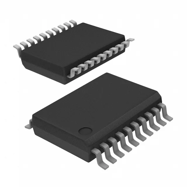
The 74FCT3807QGI is supplied in a 20-QSOP package (0.154-inch body width, 3.90 mm pitch). The QSOP footprint is smaller than a SOIC-20, which helps on dense boards.