Clock distribution for 3.3V single-ended logic
The Renesas 74FCT3807DPYGI8 is a 1:10 fanout buffer designed to distribute a single LVTTL clock or signal input to ten CMOS/TTL outputs. It handles frequencies up to 166 MHz, making it suitable for clock trees in telecom, networking, and industrial control boards where a single clock source must drive multiple loads without excessive skew or loading on the source. Supply voltage range is 3V to 3.6V, which aligns with standard 3.3V logic rails. The part is non-differential on both input and output sides, so it is intended for single-ended clock distribution only. If your design requires differential signaling (LVPECL, LVDS), this buffer will not interface directly without level translation.
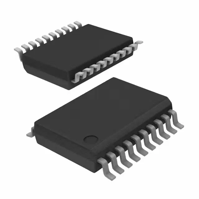
Housed in a 20-SSOP package with a 5.30 mm body width and 0.209 inch pitch, the 74FCT3807DPYGI8 is a surface-mount part. The 20-SSOP footprint is common for clock buffers and matches many existing PCB layouts.
ROHS3 compliance is confirmed, which simplifies compliance for EU and global markets.