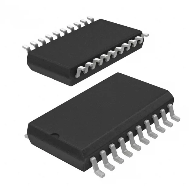
Renesas Electronics 74FCT3807ASOGI — Clock & Timing ICs

74FCT3807ASOGI Fanout Buffer, 1:10, 100 MHz, 20-SOIC

MPN74FCT3807ASOGI
End of Life

Renesas 74FCT3807ASOGI, 74FCT series, Fanout Buffer (Distribution), 1:10 ratio, 100 MHz max, LVTTL input, CMOS/TTL output, 3V to 3.6V supply, -40°C to 85°C, 20-SOIC.

$2.8Ref. price · indicative, final on quote
Packaging20-SOIC (0.295", 7.50mm Width)
StockContact for availability
MOQ1 pcs
  • 100% new & originalTraceable channels only — no refurbs, no pulls, no remarked parts.
  • Date & lot codes on quoteStated per line before you commit; label photos on request.
  • MSL-compliant ESD packingMoisture-sealed bags with indicator cards; reels photo-verified.
  • PayPal buyer protectionPay by T/T, PayPal or Payoneer — card payments covered end to end.

Specifications

74FCT3807ASOGI Technical Specifications
ParameterValue
TypeFanout Buffer (Distribution)
Series74FCT
Mounting typeSurface Mount
Voltage3V ~ 3.6V
Frequency100 MHz
Operating temperature-40°C ~ 85°C
InputLVTTL
OutputCMOS, TTL
PackageTube
Case20-SOIC (0.295\", 7.50mm Width)
Number of circuits1
Ratio - Input:Output1:10
Differential - Input:OutputNo/No

Product details

Clock fanout for single-ended trees

The Renesas 74FCT3807ASOGI is a 1:10 fanout buffer from the 74FCT series, designed to distribute a single LVTTL clock input to ten CMOS or TTL outputs. It runs from a 3V to 3.6V supply rail and handles clock rates up to 100 MHz. The industrial temperature range (-40°C to 85°C) qualifies it for motor drives, telecom line cards, and factory automation controllers.

1:10 ratio and 100 MHz ceiling

The 1:10 input-to-output ratio means one clock source drives ten loads without needing a second buffer stage. At 100 MHz the part keeps edge rates clean for most single-ended clock trees — think FPGA configuration clocks, Ethernet PHY reference clocks, or synchronous ADC sample clocks. The non-differential I/O (No/No) rules out LVPECL or LVDS fanout; this is strictly for LVTTL/CMOS rails.

20-SOIC footprint, surface-mount assembly

Housed in a 20-SOIC package (7.50 mm width), the part reflows on standard lead-free profiles. The wide-body SOIC gives good thermal contact to the PCB copper pour — useful if the buffer sits near a hot FPGA or processor. Tube shipment is the default; if your pick-and-place line feeds from tape, confirm the reel option with your distributor before committing the BOM line.

Active, no LTB watch needed

Renesas lists the 74FCT3807ASOGI as Active with ROHS3 compliance. No last-time-buy notice, no end-of-life window to track. For a production BOM that needs a single-ended clock fanout at 3.3V, this part is a stable line item — no urgency to qualify a second source unless your risk policy demands dual sourcing for all active logic.

Frequently asked questions

What is the frequency range of 74FCT3807ASOGI?

The maximum rated frequency is 100 MHz. This is the ceiling for the clock input — the output edges stay within timing spec up to that rate. For slower clocks (e.g., 25 MHz or 50 MHz) the part works fine with no derating needed.

What is 74FCT3807ASOGI's listed input and output type?

The input is LVTTL; the outputs are CMOS and TTL compatible. The part does not accept differential signals (LVPECL, LVDS) — it is strictly single-ended.