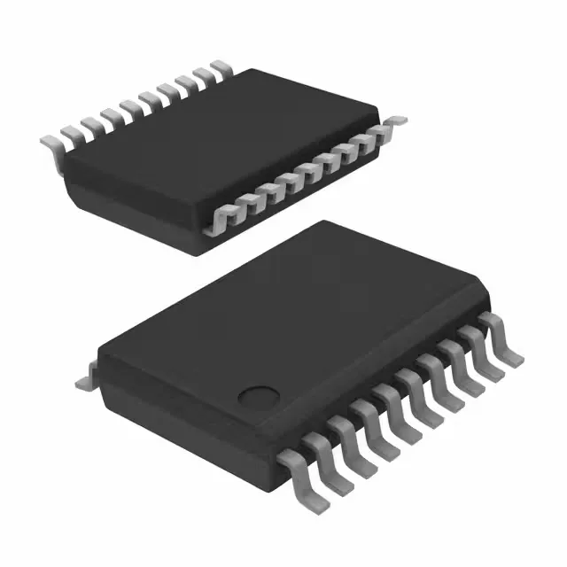
1:10 clock fanout in a 20-SSOP — what the 74FCT3807APYGI8 buys the design
The Renesas (formerly IDT) 74FCT3807APYGI8 is a 1:10 fanout buffer from the 74FCT logic family. It takes a single LVTTL clock input and distributes it to ten CMOS or TTL outputs, with a maximum frequency of 100 MHz. The 1:10 ratio is its calling card: one input fans out to ten, all with matched propagation delays, which keeps skew predictable across the clock tree. It operates from a 3V to 3.6V supply, so it sits comfortably on a 3.3V rail, and it is rated over the industrial temperature range of -40°C to 85°C. The non-inverting, non-differential topology (No/No on the differential input/output) means it is strictly a single-ended clock fanout — no LVDS or LVPECL translation on-chip.
Active and ROHS3 — no lifecycle risk for production BOMs
It is also ROHS3 compliant, which clears the environmental compliance gate for EU and other regulated markets without an exemption hunt.
Supply range and temperature — the fit decisions
The 3V to 3.6V supply range ties the part to a 3.3V nominal rail. If your board runs a 2.5V or 1.8V clock domain, you will need a level translator or a different buffer — this part's input threshold is LVTTL, so it expects the swing of a 3.3V logic signal. That is fine for most commercial and industrial environments, but for avionics or downhole tools where the junction sees extremes, you would want a wider-temperature variant or a rad-hard part. The 20-SSOP package (0.209" width, 5.30mm body) is a surface-mount footprint that routes well on a standard 4-layer PCB; the 0.025" pitch calls for a fine-pitch soldering process, not a problem for any modern assembly line.
What the 100 MHz and 1:10 ratio mean for the clock tree
The 100 MHz maximum frequency sets an upper bound on the clock speed this buffer can fan out cleanly. For a 50 MHz system clock running to ten FPGAs or ASIC inputs, the 74FCT3807APYGI8 has margin. But if your design pushes a 156.25 MHz reference clock or a 200 MHz DDR memory clock, this part will not meet the edge-rate requirement — you would need a faster buffer like the 5PB1104CMGK/W, which is rated for 200 MHz. The 1:10 ratio means one input drives ten outputs without external fanout trees or additional buffers. That saves board space and reduces component count on high-density digital boards like router line cards or server motherboards.