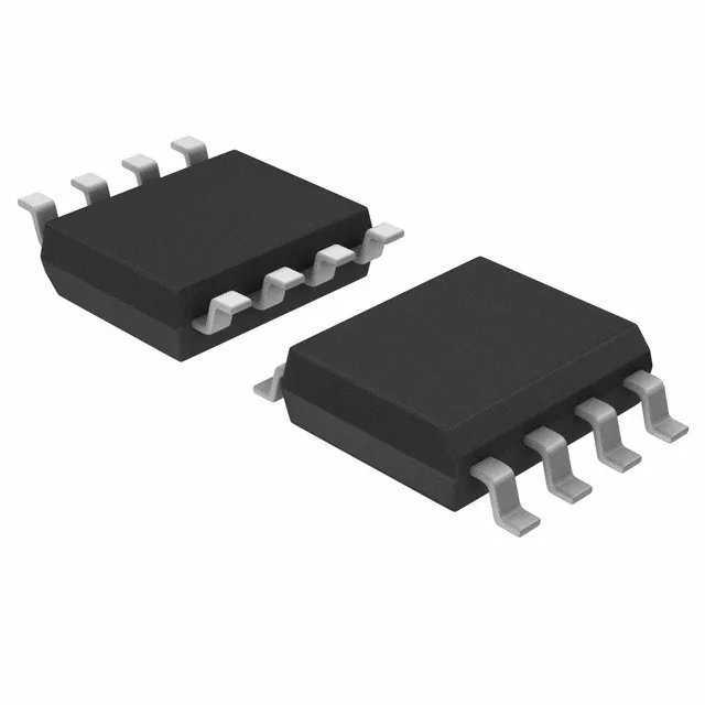
Renesas Electronics 74FCT38072SDCGI — Clock & Timing ICs

74FCT38072SDCGI Clock Buffer, 1:2 Fanout, 200 MHz, 8-SOIC

MPN74FCT38072SDCGI
End of Life

Renesas 74FCT38072SDCGI, 1:2 LVCMOS clock buffer, 200 MHz max frequency, 1.71V–3.465V supply, -40°C to 105°C, 8-SOIC package, tube.

$2.38Ref. price · indicative, final on quote
Packaging8-SOIC (0.154", 3.90mm Width)
StockContact for availability
MOQ1 pcs
  • 100% new & originalTraceable channels only — no refurbs, no pulls, no remarked parts.
  • Date & lot codes on quoteStated per line before you commit; label photos on request.
  • MSL-compliant ESD packingMoisture-sealed bags with indicator cards; reels photo-verified.
  • PayPal buyer protectionPay by T/T, PayPal or Payoneer — card payments covered end to end.

Specifications

74FCT38072SDCGI Technical Specifications
ParameterValue
TypeBuffer
Mounting typeSurface Mount
Voltage1.71V ~ 3.465V
Frequency200 MHz
Operating temperature-40°C ~ 105°C (TA)
InputLVCMOS
OutputLVCMOS
PackageTube
Case8-SOIC (0.154\", 3.90mm Width)
Number of circuits1
Ratio - Input:Output1:2
Differential - Input:OutputNo/No

Product details

1:2 LVCMOS clock buffer for 200 MHz clock trees

The Renesas 74FCT38072SDCGI is a single-circuit, 1:2 fanout clock buffer designed to distribute LVCMOS clock signals with minimal skew. It accepts one LVCMOS input and delivers two LVCMOS outputs, operating from a wide supply range of 1.71V to 3.465V, which covers 1.8V, 2.5V, and 3.3V logic rails in one BOM line. The buffer handles clock frequencies up to 200 MHz, making it suitable for mid-speed clock distribution in industrial control, motor drives, outdoor telecom, and factory automation equipment where the -40°C to 105°C industrial temperature range is required.

200 MHz and 1.71V–3.465V supply — what they mean for the clock tree

The 200 MHz maximum frequency sets the upper bound for the input clock rate; for a 100 MHz system clock this gives 2× margin, keeping output rise times clean and jitter low. The 1.71V to 3.465V supply range means the same part can be used across a multi-rail design without a separate buffer variant for each voltage — a single 74FCT38072SDCGI on the BOM covers 1.8V FPGA banks, 2.5V memory interfaces, and 3.3V peripheral logic. The 1:2 ratio is a common fanout for splitting a master clock to two loads (e.g., a processor and an FPGA), and the non-differential LVCMOS I/O avoids the termination resistor count of a differential pair.

Industrial temperature grade and 8-SOIC footprint

Rated for -40°C to 105°C ambient, this buffer is qualified for environments where the board sees elevated temperatures — motor drive cabinets, outdoor base stations, and engine-bay-adjacent electronics. The 8-SOIC package (3.90 mm body width) is a standard footprint that routes easily on two-layer boards and is compatible with common reflow profiles. The surface-mount package keeps assembly straightforward for both prototype and production runs.

Lifecycle and sourcing reality

No last-time-buy or obsolescence notice applies, so it remains a safe choice for new designs and ongoing production builds.

Frequently asked questions

Is 74FCT38072SDCGI available via RFQ confirmation?

Stock position is confirmed at quote time against an RFQ. Submit a request for current availability and lead time.

Can 74FCT38072SDCGI be used as a 1:2 fanout buffer?

Yes, the 74FCT38072SDCGI is a 1:2 fanout buffer — one LVCMOS input drives two LVCMOS outputs.

What is the difference between 74FCT38072SDCGI and 74FCT38072SOIC?

The 74FCT38072SDCGI is the specific ordering code for this 8-SOIC variant with industrial temperature range. The 'SOIC' suffix alone may refer to a different temperature grade or packaging option; verify the full order code against your BOM.