Clock fanout for low-voltage LVTTL trees
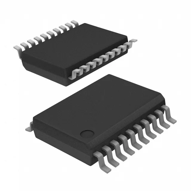
The 74FCT20807PYGI is a 1:10 fanout buffer from Renesas' 74FCT series, designed to distribute a single LVTTL clock input to ten LVTTL outputs without adding a PLL or additional buffer stages. The maximum frequency of 166 MHz sets the upper bound for the clock tree — above that, output edge rates degrade and the jitter budget tightens. The 2.3V to 2.7V supply rail means this part lives on a dedicated low-voltage plane, not a shared 3.3V or 5V bus.
Operating from 2.3V to 2.7V, the buffer is a fit for 2.5V nominal clock domains common in networking ASICs and FPGAs.
The 1:10 fanout ratio means ten output traces must be length-matched to within the skew tolerance of the downstream loads — the SSOP pitch keeps the fan-out region compact enough for a single via per trace.