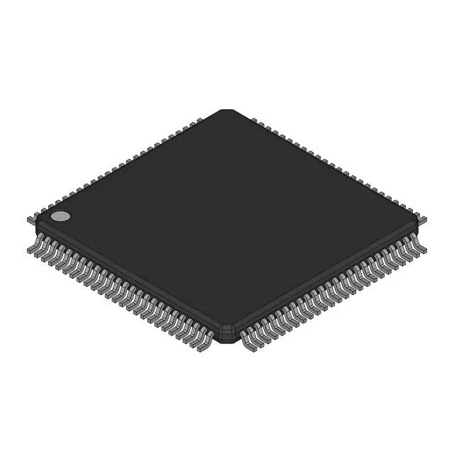
Renesas Electronics 71V65803S150PFGI — Logic ICs

71V65803S150PFGI Synchronous SRAM, 9Mbit, 150 MHz, 100-TQFP

MPN71V65803S150PFGI
End of Life

Renesas 71V65803S150PFGI, Synchronous SRAM - SDR (ZBT), 9Mbit (512K x 18), 3.8 ns access time, 150 MHz clock, Parallel interface, 3.135V-3.465V supply, -40°C to 85°C, 100-TQFP (14x14).

$14.8Ref. price · indicative, final on quote
Packaging100-LQFP
StockContact for availability
MOQ1 pcs
  • 100% new & originalTraceable channels only — no refurbs, no pulls, no remarked parts.
  • Date & lot codes on quoteStated per line before you commit; label photos on request.
  • MSL-compliant ESD packingMoisture-sealed bags with indicator cards; reels photo-verified.
  • PayPal buyer protectionPay by T/T, PayPal or Payoneer — card payments covered end to end.

Specifications

71V65803S150PFGI Technical Specifications
ParameterValue
Memory typeVolatile
Mounting typeSurface Mount
Voltage3.135V ~ 3.465V
Frequency150 MHz
Memory interfaceParallel
Operating temperature-40°C ~ 85°C (TA)
PackageBulk
TechnologySRAM - Synchronous, SDR (ZBT)
Access time3.8 ns
Memory size9Mbit
Memory formatSRAM
Case100-LQFP
Memory organization512K x 18

Product details

Synchronous SRAM for high-throughput cache and buffer applications

It delivers a 150 MHz clock frequency with a 3.8 ns access time, making it suited for networking equipment, base stations, and telecom line cards where deterministic read-write throughput matters.

150 MHz clock and 3.8 ns access — what drives the timing budget

At 150 MHz the part cycles at 6.67 ns, and the 3.8 ns access time leaves roughly 2.9 ns of setup/hold margin for the controller. That margin shrinks with trace delay and clock skew, so the PCB layout engineer should keep the SRAM close to the memory controller and match trace lengths within 10 mm. The ZBT architecture eliminates the dead bus cycle between read and write transitions, which matters for back-to-back throughput in packet processing and DMA engines.

The 18-bit word width (16 data bits plus 2 parity/ECC bits) is common in telecom framing and network processor applications. If the design uses a 32-bit or 64-bit memory bus, two or four of these parts populate the array. The 9Mbit total density suits moderate-sized lookup tables, packet buffers, and trace caches where SRAM speed is needed but DRAM latency is unacceptable.

Supply and temperature range for the environment

The 100-TQFP (14x14 mm) package with 0.5 mm pitch is a common footprint for mid-density SRAM, and the surface-mount assembly is straightforward for standard reflow profiles.

Frequently asked questions

Is 71V65803S150PFGI obsolete?

No, the manufacturer lists this part with an active lifecycle status. There is no current end-of-life notification for this order code.

What is the memory organization and interface of 71V65803S150PFGI?

The SDR ZBT architecture supports back-to-back read and write cycles without dead bus cycles.

Is 71V65803S150PFGI RoHS compliant?

The part is listed with the PFGI suffix, which indicates a lead-free (RoHS-compliant) finish per Renesas standard part numbering. Confirm the latest compliance certificate with the supplier at quote time.