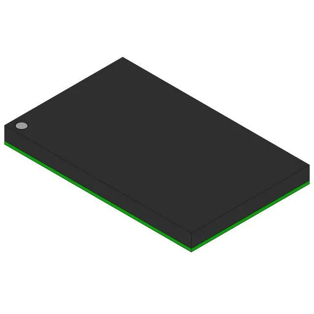
Synchronous ZBT SRAM — 8 ns access, 256K x 36 organisation
The Renesas 71V65703S80BG is a 9 Mbit synchronous SRAM organised as 256K x 36, using a Zero Bus Turnaround (ZBT) architecture that eliminates dead cycles when switching between read and write operations. The 8 ns access time supports bus clocking up to 133 MHz class without wait states, provided the PCB trace delay and load capacitance stay within the datasheet derating curves. The 36-bit wide datapath matches directly to 36-bit DSP or network processor memory buses, saving the external byte-lane mux logic a narrower part would need.
Supply rail and temperature grade — what fits
Not rated for industrial enclosures, motor drives, or outdoor deployments without additional thermal qualification.
119-ball PBGA — layout and reflow considerations
The 119-PBGA package measures 14 x 22 mm with a fine-pitch ball array. The BGA footprint demands a via-in-pad or dogbone fan-out strategy for the 36 data lines plus address and control signals. Plan for a 4-layer minimum PCB with a dedicated 3.3 V plane and solid ground pour under the package. The reflow profile should follow the JEDEC MSL rating for the part — verify the moisture sensitivity level before the bake decision if the bag seal has been broken.