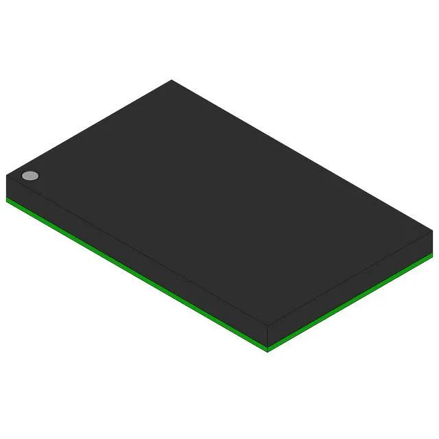
7.5 ns ZBT SRAM in a 119-ball BGA — what this part is
The Renesas 71V65703S75BGG is a 9 Mbit synchronous SRAM organized as 256K x 36, built on a Zero Bus Turnaround (ZBT) architecture. It presents a 7.5 ns access time from clock edge to data valid, which is the headline parameter for timing closure on a high-throughput datapath. The 36-bit word width maps cleanly to a 32-bit data bus plus parity or ECC nibble — common in networking packet buffers and telecom line-card applications. The part operates from a 3.135 V to 3.465 V supply and is rated over the commercial temperature range of 0°C to 70°C.
7.5 ns access — timing margin on a 100+ MHz bus
A 7.5 ns access time means the SRAM can support clock frequencies up to roughly 133 MHz while leaving a few nanoseconds of setup/hold margin for the controller. For a system architect, that margin is the difference between a first-pass layout and a respin to add pipeline stages. The ZBT protocol eliminates the dead bus cycle between read and write turns, so back-to-back throughput is sustained at the full clock rate — no idle cycle penalty when switching direction.
119-PBGA (14x22) — layout and rework notes
The 119-ball BGA on a 14 mm x 22 mm substrate is a fine-pitch array. For the PCB layout engineer, that means via-in-pad or microvia fanout under the body unless the board stackup allows a dogbone escape on the outer rows. The part is surface-mount only. The commercial temperature rating (0°C to 70°C) limits this to indoor, conditioned environments; it is not a fit for outdoor telecom cabinets or factory-floor motor drives.