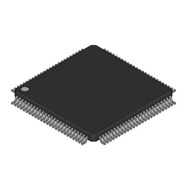
Renesas Electronics 71V65603S150PFG — DC-DC Power Modules

71V65603S150PFG 9Mbit ZBT SRAM, 150 MHz, 3.8 ns, 100-TQFP

MPN71V65603S150PFG
End of Life

Renesas 71V65603S150PFG, 9Mbit Synchronous SRAM, ZBT (Zero Bus Turnaround), 150 MHz, 3.8 ns access time, 256K x 36, Parallel interface, 3.135V–3.465V supply, 0°C–70°C, 100-TQFP (14x14), Surface Mount.

$10.68Ref. price · indicative, final on quote
Packaging100-LQFP
StockContact for availability
MOQ1 pcs
  • 100% new & originalTraceable channels only — no refurbs, no pulls, no remarked parts.
  • Date & lot codes on quoteStated per line before you commit; label photos on request.
  • MSL-compliant ESD packingMoisture-sealed bags with indicator cards; reels photo-verified.
  • PayPal buyer protectionPay by T/T, PayPal or Payoneer — card payments covered end to end.

Specifications

71V65603S150PFG Technical Specifications
ParameterValue
Memory typeVolatile
Mounting typeSurface Mount
Voltage3.135V ~ 3.465V
Frequency150 MHz
Memory interfaceParallel
Operating temperature0°C ~ 70°C (TA)
PackageBulk
TechnologySRAM - Synchronous, SDR (ZBT)
Access time3.8 ns
Memory size9Mbit
Memory formatSRAM
Case100-LQFP
Memory organization256K x 36

Product details

9 Mbit ZBT SRAM – what this part is and where it fits

The Renesas 71V65603S150PFG is a 9 Mbit synchronous SRAM built on Zero Bus Turnaround (ZBT) technology, organized as 256K x 36 bits. It runs at a 150 MHz clock with a 3.8 ns access time, feeding a parallel interface that eliminates the dead bus cycle between read and write operations. This makes it a natural fit for high-throughput datapaths in networking equipment, baseband processing, and DSP arrays where every clock cycle of bus utilization counts. The commercial temperature range (0°C to 70°C) confines it to controlled indoor environments — server rooms, telecom central offices, test equipment — not unheated enclosures or outdoor cabinets.

3.8 ns access time at 150 MHz – timing margin in practice

The 3.8 ns access time is the delay from address assertion to data valid on the bus. At a 150 MHz clock, that leaves margin for the receiving FPGA or ASIC.

Lifecycle and sourcing posture

The 71V65603S150PFG carries an Active lifecycle status. For production BOM lines, this means no near-term obsolescence risk. The package marking and date-code consistency should be verified on receipt — the 100-TQFP form factor is a known target for re-marking in the gray market, so lot traceability back to the authorized channel is worth documenting.

Frequently asked questions

Does 71V65603S150PFG support ZBT (Zero Bus Turnaround) mode?

Yes, the part uses Synchronous SDR (ZBT) technology, which eliminates the dead bus cycle between read and write operations for continuous throughput.