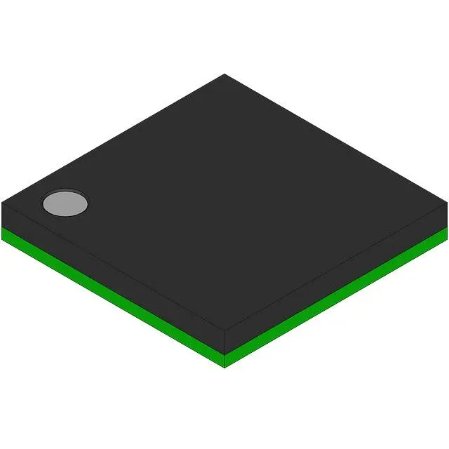
10 ns asynchronous SRAM — the fit check for a fast cache line
The 10 ns figure is the cycle time from address change to valid data out — a 100 MHz bus can read it back-to-back with zero dead cycles, but a 133 MHz or faster controller will need a wait state or a pipelined SRAM. The parallel interface is straightforward: assert chip select, address lines, and output enable; data appears on the bus 10 ns later. No refresh logic needed — it's truly asynchronous, so it drops into any memory controller that supports a basic SRAM handshake.
Package and supply — the board-level constraints
The 71V416L10BE comes in a 48-TFBGA (48-CABGA) package with a 9x9 mm body. That's a fine-pitch BGA — 0.75 mm ball pitch typical for this form factor — so the PCB needs via-in-pad or microvias for routing, and rework requires a hot-air station with a BGA nozzle and a stencil for the solder paste.
That removes the immediate obsolescence risk for a BOM line.