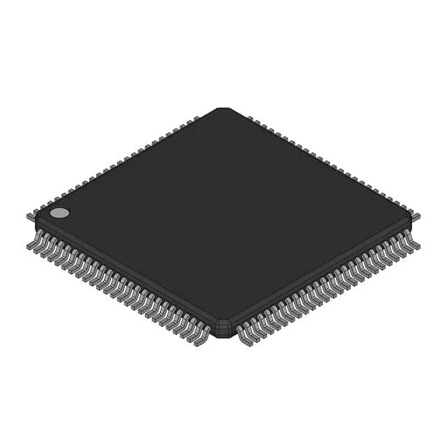
The Renesas 71V3577S80PFGI is a 4.5 Mbit synchronous SRAM organized as 128K x 36 bits, with a parallel interface and a 100 MHz clock that delivers an 8 ns access time.
8 ns access and 100 MHz clock — timing margin for the controller
In a typical FPGA or ASIC memory controller, the combination leaves enough setup-and-hold margin to avoid wait states at 100 MHz, provided the board trace lengths are matched within a few inches. If the controller runs at a slower clock, the access time gives even more slack for signal-integrity derating across temperature.
128K x 36 organization — why the extra bits matter
A 36-bit word width is wider than the common x32 or x18 configurations. The extra four bits can carry byte parity or a nibble of ECC syndrome without stealing data bandwidth.
The 100-pin LQFP (also specified as 100-TQFP 14x14 mm) is a common surface-mount footprint that reflows easily with standard lead-free profiles. A local LDO or a well-regulated DC-DC is recommended if the system bus voltage wanders.