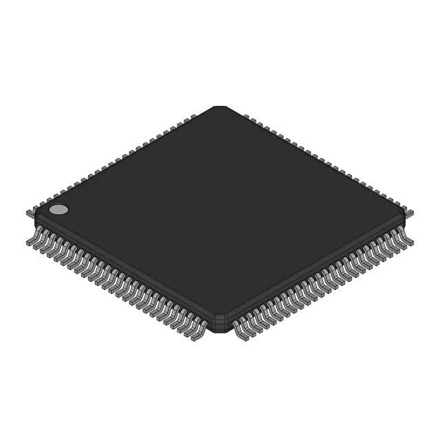
256K x 18 synchronous SRAM with Zero Bus Turnaround
The Renesas 71V3558S100PFG is a 4.5 Mbit synchronous SRAM organized as 256K x 18 bits, using ZBT (Zero Bus Turnaround) architecture to eliminate dead cycles between read and write operations. The 5 ns access time means the memory controller has a full clock cycle to capture data at 100 MHz, leaving timing margin for board trace delays and signal-integrity effects. The 18-bit data bus (16 data + 2 parity/byte-write) suits designs needing byte-level write control without external logic.
100 MHz clock and bus turnaround
At 100 MHz the ZBT pipeline delivers back-to-back read-write throughput without the dead cycle that conventional synchronous SRAMs insert. This matters for networking packet buffers, DSP coefficient tables, or any application where the bus direction flips every cycle.
No extended temperature or AEC-Q qualification is listed.
The surface-mount package is compatible with standard reflow processes. No exposed thermal pad; junction temperature is managed through the leadframe and board copper.
Listed as Active. For BOM planning, no immediate replacement risk exists.