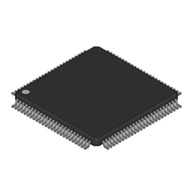
Renesas Electronics 71V3557S85PFG — Logic ICs

71V3557S85PFG SRAM, 4.5 Mbit, 8.5 ns, 100-TQFP

MPN71V3557S85PFG
End of Life

Renesas 71V3557S85PFG, Synchronous SRAM (ZBT), 4.5 Mbit (128K x 36), 8.5 ns access time, Parallel interface, 3.135V–3.465V supply, 0°C to 70°C, 100-TQFP.

$4.67Ref. price · indicative, final on quote
Packaging100-LQFP
StockContact for availability
MOQ1 pcs
  • 100% new & originalTraceable channels only — no refurbs, no pulls, no remarked parts.
  • Date & lot codes on quoteStated per line before you commit; label photos on request.
  • MSL-compliant ESD packingMoisture-sealed bags with indicator cards; reels photo-verified.
  • PayPal buyer protectionPay by T/T, PayPal or Payoneer — card payments covered end to end.

Specifications

71V3557S85PFG Technical Specifications
ParameterValue
Memory typeVolatile
Mounting typeSurface Mount
Voltage3.135V ~ 3.465V
Memory interfaceParallel
Operating temperature0°C ~ 70°C (TA)
PackageBulk
TechnologySRAM - Synchronous, SDR (ZBT)
Access time8.5 ns
Memory size4.5Mbit
Memory formatSRAM
Case100-LQFP
Memory organization128K x 36

Product details

8.5 ns ZBT SRAM for high-throughput data paths

The Renesas 71V3557S85PFG is a 4.5 Mbit synchronous SRAM organized as 128K x 36 bits, with a zero-bus-turnaround (ZBT) architecture that eliminates dead cycles when switching between read and write. The 8.5 ns access time lets it keep pace with a 100+ MHz bus in a pipelined system, making it a common choice for network buffers, DSP scratchpads, and cache tag stores where every cycle of throughput matters.

128K x 36 organization — why the extra width

The 36-bit word width is wider than the more common x32 or x18 SRAMs. That extra nibble per word is often used to carry a parity or ECC check bit alongside a 32-bit data bus, saving an external logic layer. In a DSP or FPGA-based design, it also allows packing two 18-bit samples per access, effectively doubling the data rate for a given clock frequency.

Package and footprint

Housed in a 100-pin TQFP (14x14 mm body, 0.5 mm pitch), the 71V3557S85PFG is a surface-mount part intended for reflow assembly. The fine pitch demands careful solder-paste stencil design and a controlled reflow profile to avoid bridging. The package is MSL 3 per JEDEC — if the moisture-barrier bag has been open longer than the floor-life window, a bake-out is required before reflow to prevent popcorning.

Frequently asked questions

Can 71V3557S85PFG be replaced with 71V3557S80PFG?

The 71V3557S80PFG is a faster variant (8.0 ns access time) in the same package and pinout. It is a drop-in replacement if the system timing budget can accommodate the slightly faster access — verify the setup/hold margins at the controller side before swapping.

What is the access time of 71V3557S85PFG?

The access time is 8.5 ns. This is the time from address assertion to valid data on the output pins, and it determines the maximum bus clock frequency the memory can support in a synchronous pipeline.

Is 71V3557S85PFG RoHS compliant?

The part is lead-free and RoHS compliant per the manufacturer's standard marking. The PFG suffix indicates a lead-free (RoHS) finish on the 100-TQFP package.