Synchronous ZBT SRAM at 133 MHz — what the pipeline buys you
The Renesas 71V3556SA133BG is a 4.5 Mbit synchronous SRAM organized 128K x 36, using a Zero Bus Turnaround (ZBT) architecture that eliminates the dead cycle when switching between read and write. It clocks at 133 MHz with a 4.2 ns access time from the clock edge, which means back-to-back transactions at full bus rate with no wait-state insertion for direction changes. The 36-bit word width maps naturally to a 32-bit data bus plus parity or ECC lane, common in network packet buffers, DSP ping-pong memories, and high-speed cache applications.
Timing margin and the 4.2 ns access window
At 133 MHz the clock period is 7.5 ns. The 4.2 ns access time leaves about 3.3 ns for the controller to capture data before the next clock edge. That budget covers PCB trace delay, input capacitance, and setup time of the receiving FPGA or ASIC. If the design uses a 133 MHz memory controller, verify the input setup requirement against this window — a 3.3 ns margin is comfortable for short traces on a moderate-density board, but a heavily loaded bus or long routing may force a speed-grade bump or a slower clock. The ZBT pipeline adds one cycle of latency on the first access, but subsequent pipelined reads and writes sustain full throughput.
Package and supply rail — footprint and decoupling notes
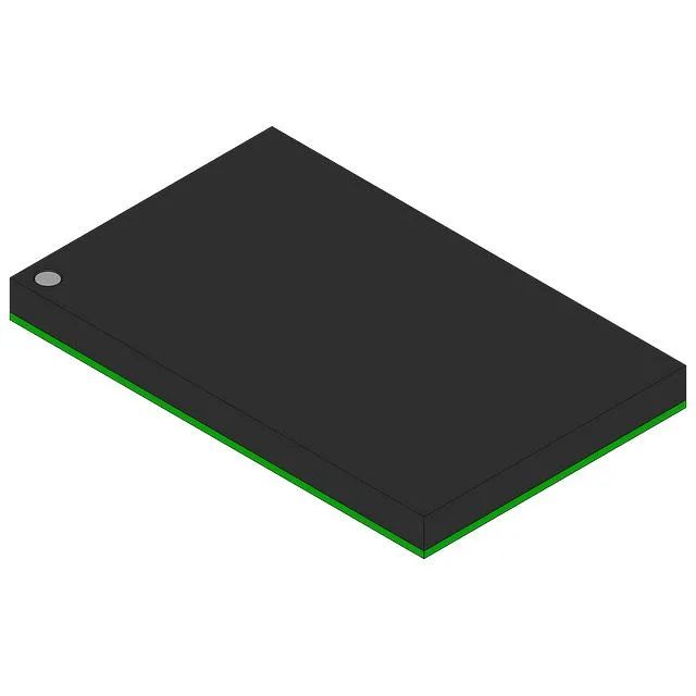
The 119-ball PBGA measures 14x22 mm, a standard fine-pitch BGA footprint. Decoupling should follow the manufacturer's recommended capacitor placement — multiple 0.1 µF ceramics distributed near the supply balls, plus a bulk capacitor per the layout guide. For extended temperature or industrial use, check the -I or -B temperature grade variants in the family.
Active lifecycle — no imminent EOL, suitable for production
For dual-sourcing or drop-in replacement, the 71V3556SA133BG is a standard density and speed grade in the 71V3556 family; other speed grades (e.g., 100 MHz or 166 MHz) share the same 119-PBGA footprint and pinout, allowing a speed upgrade without a board respin.