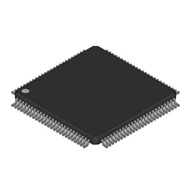
What this synchronous SRAM is and who needs it
The Renesas 71V3556S166PFG is a 4.5Mbit synchronous SRAM organized as 128K x 36, using a Zero Bus Turnaround (ZBT) architecture that eliminates dead cycles between read and write operations.
166 MHz and 3.5 ns — what the speed ratings mean for bus timing
The 166 MHz clock frequency and 3.5 ns access time are the headline numbers that decide whether this part can sit on a high-speed memory bus without wait states. A 166 MHz bus has a 6 ns cycle period; a 3.5 ns access time leaves about 2.5 ns of margin after address setup and hold for the SRAM to present valid data — tight but workable with controlled-impedance routing and matched trace lengths. If the processor's memory controller expects a 3.3V SRAM with a 3.5 ns tAA, this part fits that slot. The ZBT pipeline means back-to-back reads and writes happen every clock cycle with no idle turn-around, which is what the network-equipment designers chose it for.