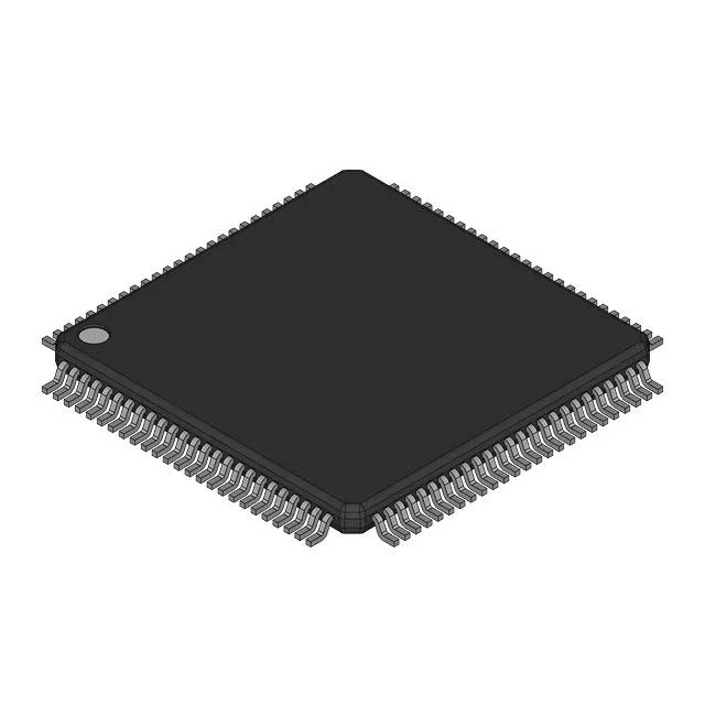
Renesas Electronics 71V2546S150PFG — Logic ICs

71V2546S150PFG 4.5Mbit Synchronous SRAM, 3.8 ns, 150 MHz

MPN71V2546S150PFG
End of Life

Renesas 71V2546S150PFG, 4.5Mbit Synchronous SRAM (ZBT), 128K x 36, 3.8 ns access time, 150 MHz clock, Parallel interface, 3.135V–3.465V supply, 0°C to 70°C, 100-TQFP (14x14).

$4.11Ref. price · indicative, final on quote
Packaging100-LQFP
StockContact for availability
MOQ1 pcs
  • 100% new & originalTraceable channels only — no refurbs, no pulls, no remarked parts.
  • Date & lot codes on quoteStated per line before you commit; label photos on request.
  • MSL-compliant ESD packingMoisture-sealed bags with indicator cards; reels photo-verified.
  • PayPal buyer protectionPay by T/T, PayPal or Payoneer — card payments covered end to end.

Specifications

71V2546S150PFG Technical Specifications
ParameterValue
Memory typeVolatile
Mounting typeSurface Mount
Voltage3.135V ~ 3.465V
Frequency150 MHz
Memory interfaceParallel
Operating temperature0°C ~ 70°C (TA)
PackageBulk
TechnologySRAM - Synchronous, SDR (ZBT)
Access time3.8 ns
Memory size4.5Mbit
Memory formatSRAM
Case100-LQFP
Memory organization128K x 36

Product details

The Renesas 71V2546S150PFG is a 4.5 Mbit synchronous SRAM using the ZBT (Zero Bus Turnaround) architecture, organized 128K x 36. The 3.8 ns access time at a 150 MHz clock means the part can deliver a 36-bit word every clock cycle with no dead cycles between read and write turns — critical for cache-line fills, packet buffers, or DSP coefficient tables where back-to-back throughput matters more than raw density.

Supply and temperature — where it runs

Not rated for industrial or automotive under-hood use.

Package and footprint

Housed in a 100-pin TQFP (14x14 mm) — a fine-pitch surface-mount package that reflows on standard SMT lines. No exposed thermal pad, so all heat dissipates through the leads; keep the ambient airflow adequate if running sustained back-to-back bursts at 150 MHz. The 100-TQFP footprint is shared across the 71V2546 family, so a board laid out for the 150 MHz speed grade can also accept the 133 MHz or 200 MHz variants without a layout change.

Frequently asked questions

What is the access time of 71V2546S150PFG?

The access time is 3.8 ns, which at a 150 MHz clock gives a single-cycle read or write latency — no wait states needed for a processor running at that speed.

Can 71V2546S150PFG be used with a 3.3V supply?

Yes.

Is 71V2546S150PFG a direct replacement for 71V2546S150BFG?

The BFG suffix typically indicates a different package (often BGA). The PFG is a 100-TQFP. They are not pin-compatible — the package footprint differs. Verify the board's target footprint before substituting.