Dual-port asynchronous SRAM — 32 Kbit, 20 ns, 5 V
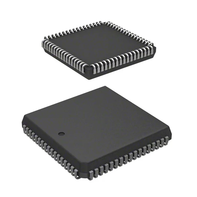
The Renesas 7143LA20JG is a 32 Kbit dual-port asynchronous SRAM organised as 2K × 16 bits, with a 20 ns access time and a 4.5 V to 5.5 V supply range. It is built for applications where two independent buses — typically a DSP and a microcontroller, or two processors — need simultaneous read/write access to a shared memory block without external arbitration logic. The 16-bit word width maps directly onto a 16-bit data bus, saving byte-lane multiplexing. The part is rated for commercial temperature environments (0°C to 70°C) and comes in a 68-lead PLCC with J-leads, a surface-mount footprint common in mid-1990s through 2000s designs.
20 ns access time — bus timing margin
It is not rated for industrial environments.
The 68-PLCC package (24.21 × 24.21 mm body) uses J-leads. It is a surface-mount package that can be soldered directly or socketed.
For BOM planning, there is no immediate obsolescence risk, but dual-port SRAMs are a shrinking market — most new designs migrate to dual-port RAM in FPGAs or to QDR/DDR SRAM. If the design is locked to this footprint, confirm supply annually.