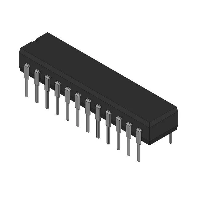
Renesas Electronics 6116LA15TPG — Memory (DRAM / SRAM / Flash / EEPROM)

6116LA15TPG 16Kbit SRAM, 15 ns Access, DIP-24

MPN6116LA15TPG
End of Life

Integrated Device Technology 6116LA15TPG, 16Kbit (2K x 8) Asynchronous SRAM, 15 ns access time, 4.5V ~ 5.5V supply, -40°C to 85°C, 24-DIP (0.300", 7.62mm) through-hole package.

$2.8Ref. price · indicative, final on quote
Packaging24-DIP (0.300", 7.62mm)
StockContact for availability
MOQ1 pcs
  • 100% new & originalTraceable channels only — no refurbs, no pulls, no remarked parts.
  • Date & lot codes on quoteStated per line before you commit; label photos on request.
  • MSL-compliant ESD packingMoisture-sealed bags with indicator cards; reels photo-verified.
  • PayPal buyer protectionPay by T/T, PayPal or Payoneer — card payments covered end to end.

Specifications

6116LA15TPG Technical Specifications
ParameterValue
Memory typeVolatile
Mounting typeThrough Hole
Voltage4.5V ~ 5.5V
Memory interfaceParallel
Operating temperature-40°C ~ 85°C (TA)
PackageBulk
TechnologySRAM - Asynchronous
Access time15 ns
Memory size16Kbit
Memory formatSRAM
Case24-DIP (0.300\", 7.62mm)
Memory organization2K x 8
Write cycle time - word, page15ns

Product details

15 ns asynchronous SRAM for legacy bus timing

The 6116LA15TPG is a 16Kbit (2K x 8) asynchronous SRAM from Integrated Device Technology, organized as 2K words of 8 bits each. Its 15 ns access time determines how fast the memory can deliver data after the address lines settle.

Industrial temperature and through-hole package

Rated for -40°C to 85°C, this SRAM is suited for unheated enclosures, outdoor telecom cabinets, and factory-floor controllers where ambient temperature swings exceed commercial-grade limits. The 24-pin DIP (0.300" row spacing) is a through-hole package — it plugs directly into a socket or solders into plated-through holes on a PCB. For field-service replacements on legacy boards, the DIP footprint allows quick socket swaps without reflow equipment.

15 ns write cycle — same speed as read

The write cycle time matches the read access time at 15 ns, so the memory can sustain back-to-back read and write operations at the same bus speed without wait states. This simplifies timing closure for controllers that use a single memory cycle for both directions.

Frequently asked questions

What is the access time of 6116LA15TPG?

The access time is 15 ns. This is the time from address valid to data valid on the outputs, and it matches the write cycle time of 15 ns.

Can 6116LA15TPG be used as a replacement for 6116LA20TPG?

Yes, it is a direct speed-grade upgrade — same pinout, same 2K x 8 organization, same package. The 15 ns version is faster than the 20 ns variant, so it can replace the slower part in any design that meets the 15 ns timing budget.

What is the pinout of 6116LA15TPG?

It follows the standard JEDEC 24-pin DIP pinout for 2K x 8 asynchronous SRAM: address lines A0–A10, data lines DQ0–DQ7, chip enable (CE), output enable (OE), write enable (WE), VCC, and GND. The pinout is identical across the 6116 family.