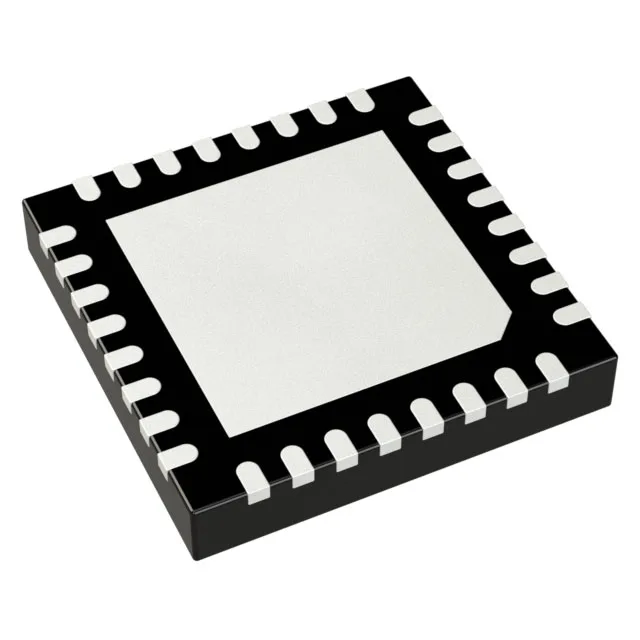
Renesas Electronics 5V49EE902NLGI — Clock & Timing ICs

5V49EE902NLGI VersaClock III Clock Generator, 500 MHz

MPN5V49EE902NLGI
End of Life

Renesas VersaClock® III 5V49EE902NLGI clock generator and multiplexer, PLL with bypass, 2:7 input:output ratio, 500 MHz max frequency, HCSL/LVCMOS/LVDS/LVPECL/LVTTL outputs, 3.135V–3.465V supply, -40°C to 85°C, 32-VFQFPN (5x5 mm).

$10.97Ref. price · indicative, final on quote
Packaging32-VFQFN Exposed Pad
StockContact for availability
MOQ1 pcs
  • 100% new & originalTraceable channels only — no refurbs, no pulls, no remarked parts.
  • Date & lot codes on quoteStated per line before you commit; label photos on request.
  • MSL-compliant ESD packingMoisture-sealed bags with indicator cards; reels photo-verified.
  • PayPal buyer protectionPay by T/T, PayPal or Payoneer — card payments covered end to end.

Specifications

5V49EE902NLGI Technical Specifications
ParameterValue
TypeClock Generator, Multiplexer
SeriesVersaClock® III
Mounting typeSurface Mount
Voltage3.135V ~ 3.465V
Frequency500MHz
Operating temperature-40°C ~ 85°C
PLLYes with Bypass
InputLVCMOS, LVTTL, Crystal
OutputHCSL, LVCMOS, LVDS, LVPECL, LVTTL
PackageTray
Case32-VFQFN Exposed Pad
Divider (Multiplier)Yes/Yes
Number of circuits1
Ratio - Input:Output2:7
Differential - Input:OutputNo/Yes

Product details

What this clock generator does on the board

The Renesas 5V49EE902NLGI is a VersaClock® III clock generator and multiplexer that takes up to two inputs — LVCMOS, LVTTL, or a crystal — and produces up to seven output clocks across five differential or single-ended standards: HCSL, LVCMOS, LVDS, LVPECL, and LVTTL. The on-chip PLL includes a bypass mode. Maximum output frequency is 500 MHz. Supply voltage is 3.135 V to 3.465 V.

Output format flexibility — one part, many standards

The output bank supports HCSL, LVDS, LVPECL, LVCMOS, and LVTTL. The 2:7 input-to-output ratio gives seven independent clock copies from two source selections.

Industrial temperature and supply tolerance

Rated for -40°C to 85°C. Supply voltage is 3.135 V to 3.465 V. Package is 32-VFQFPN (5x5 mm).

Lifecycle and sourcing posture

Renesas lists the 5V49EE902NLGI as Active and ROHS3 compliant. No end-of-life notice or last-time-buy schedule is in effect, so the part is safe to specify for new production builds.

Frequently asked questions

What output types does 5V49EE902NLGI support?

The 5V49EE902NLGI outputs HCSL, LVCMOS, LVDS, LVPECL, and LVTTL. This covers PCIe, SerDes, and general-purpose logic clocking from a single device.

What is the maximum output frequency of 5V49EE902NLGI?

The maximum output frequency is 500 MHz, suitable for PCIe Gen1/2/3 reference clocks, Ethernet SerDes, and FPGA transceiver reference tiers.

What is the PLL bypass feature on 5V49EE902NLGI?

The PLL includes a bypass mode, allowing the input clock to pass through without phase-locking. This is useful when jitter cleaning is not needed or for test/debug scenarios.

What is the closest pin-compatible alternative to 5V49EE902NLGI?

Within the VersaClock III family, other members share the same 32-VFQFPN footprint and supply voltage but differ in output count or PLL configuration. Verify the specific output and frequency requirements against the family selector guide before substituting.