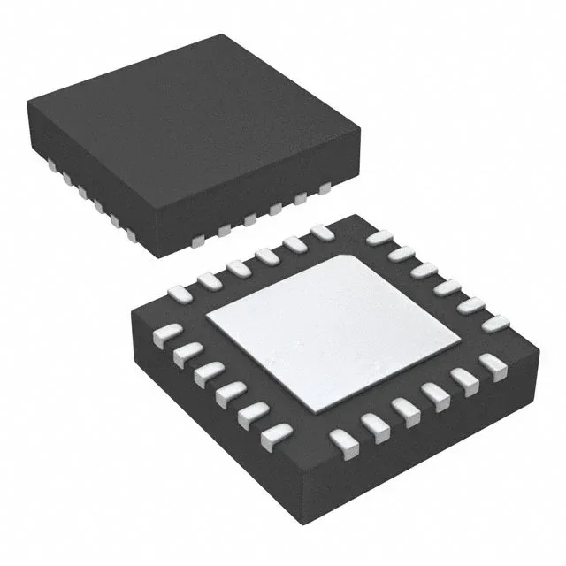
Renesas Electronics 5V49EE503NLGI — Clock & Timing ICs

5V49EE503NLGI Clock Generator

MPN5V49EE503NLGI
End of Life

Renesas VersaClock® III, Clock Generator, Multiplexer, PLL Yes with Bypass, 200MHz max, 2:5 I/O, 3.3V supply, -40°C to 85°C, 24-QFN (4x4)

$6.18Ref. price · indicative, final on quote
Packaging24-VFQFN Exposed Pad
StockContact for availability
MOQ1 pcs
  • 100% new & originalTraceable channels only — no refurbs, no pulls, no remarked parts.
  • Date & lot codes on quoteStated per line before you commit; label photos on request.
  • MSL-compliant ESD packingMoisture-sealed bags with indicator cards; reels photo-verified.
  • PayPal buyer protectionPay by T/T, PayPal or Payoneer — card payments covered end to end.

Specifications

5V49EE503NLGI Technical Specifications
ParameterValue
TypeClock Generator, Multiplexer
SeriesVersaClock® III
Mounting typeSurface Mount
Voltage3.135V ~ 3.465V
Frequency200MHz
Operating temperature-40°C ~ 85°C
PLLYes with Bypass
InputLVCMOS, LVTTL, Crystal
OutputLVCMOS, LVTTL
PackageTray
Case24-VFQFN Exposed Pad
Divider (Multiplier)Yes/Yes
Number of circuits1
Ratio - Input:Output2:5
Differential - Input:OutputNo/No

Product details

Package and mounting

The 5V49EE503NLGI is a clock generator and multiplexer from Renesas' VersaClock® III family. Its PLL can be bypassed, which means you get a clean reference path when the PLL's jitter isn't needed — useful for low-jitter fan-out or for feeding a downstream PLL that does its own cleanup. The PLL itself synthesizes up to 200 MHz from a crystal or LVCMOS input, and the 2:5 input-to-output ratio lets you route one of two input sources to five output banks.

200 MHz ceiling and 3.3V rail tolerance

The 200 MHz maximum output frequency covers most FPGA reference clocks, Ethernet PHY MACs, and SoC core clocks. The supply range is 3.135V to 3.465V — that's a 3.3V nominal rail with ±5% tolerance. If your board's 3.3V regulator holds within that band, no extra LDO is needed. The outputs are LVCMOS / LVTTL, so they drive standard digital loads without level translation.

Active production — no LTB clock ticking

Renesas lists the 5V49EE503NLGI as Active. The part ships in a tray, surface-mount in a 24-VFQFN exposed pad package with a 4x4 mm body. ROHS3 compliant.

The 24-QFN package with exposed pad needs a thermal via array under the paddle to pull heat into the ground plane — the datasheet's recommended footprint is worth following for reliable solder-joint life across the temperature sweep.

Frequently asked questions

What is the difference between 5V49EE503NLGI and 5V49EE503NLG?

The 'NLG' variant may have a different temperature grade or package code — confirm the full part number against your BOM's temperature requirement before substituting.

Can the 5V49EE503NLGI be used in a 3.3V design?

Yes. The supply voltage range is 3.135V to 3.465V, which covers a nominal 3.3V rail with ±5% tolerance. The outputs are LVCMOS / LVTTL, so they drive 3.3V logic directly.

Does the 5V49EE503NLGI require an external crystal?

It accepts a crystal as one of its input options, but also accepts LVCMOS or LVTTL clock inputs. If you use a crystal, it must be connected to the on-chip oscillator — the datasheet specifies the crystal load capacitance and ESR range.