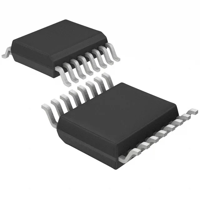
200 MHz PCIe reference clock with spread-spectrum modulation
The 5V41235PGGI is a Renesas PLL-based clock generator built for PCI Express reference clock trees. It accepts a single-ended clock or crystal input and produces two differential HCSL or LVDS outputs at up to 200 MHz — the 1:2 fanout covers the common case of clocking a root complex and one downstream device from one source. The integrated spread-spectrum modulation reduces peak EMI on the PCIe reference clock trace, which can relax the board-layer stack-up constraints in a dense multi-lane backplane. The 3.135 V to 3.465 V supply rail matches the standard 3.3 V PCIe power plane, so no additional regulator is needed for the clock generator.
For a base station, outdoor small-cell, or industrial backplane that sees seasonal temperature swings, the I-grade margin avoids clock-deviation drift at the PCIe reference. The differential HCSL/LVDS output pair traces need 100 Ω differential impedance to the receiver — the tight 3.3 V supply tolerance (3.135 V to 3.465 V) keeps the output swing within the PCIe common-mode range without an external voltage reference.
Active lifecycle — no design-in risk
ROHS3 compliant (lead-free, no exemptions), it passes the material declaration requirements for EU and UKCA markets without a waiver.