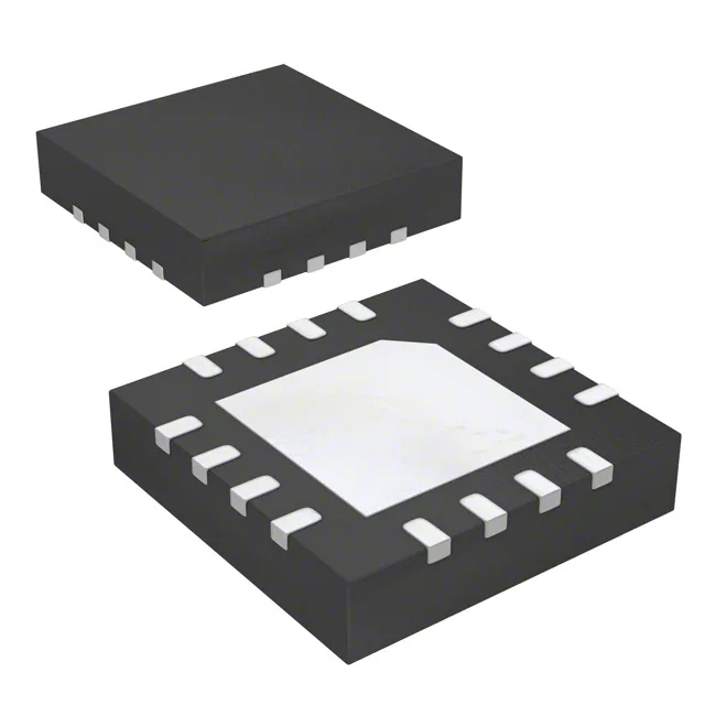
Renesas Electronics 5V41234NLG — Clock & Timing ICs

5V41234NLG PCIe Clock Generator, PLL, 100 MHz, 16-VFQFPN

MPN5V41234NLG
End of Life

Renesas 5V41234NLG clock generator IC, PLL Yes, input LVCMOS/Crystal, output HCSL/LVDS, 100 MHz max, 1:1 ratio, 3.135V-3.465V supply, 0°C to 70°C, 16-VFQFN Exposed Pad, Tray.

$3.35Ref. price · indicative, final on quote
Packaging16-VFQFN Exposed Pad
StockContact for availability
MOQ1 pcs
  • 100% new & originalTraceable channels only — no refurbs, no pulls, no remarked parts.
  • Date & lot codes on quoteStated per line before you commit; label photos on request.
  • MSL-compliant ESD packingMoisture-sealed bags with indicator cards; reels photo-verified.
  • PayPal buyer protectionPay by T/T, PayPal or Payoneer — card payments covered end to end.

Specifications

5V41234NLG Technical Specifications
ParameterValue
Mounting typeSurface Mount
Voltage3.135V ~ 3.465V
Frequency100MHz
Operating temperature0°C ~ 70°C
PLLYes
InputLVCMOS, Crystal
OutputHCSL, LVDS
PackageTray
Main purposePCI Express (PCIe)
Case16-VFQFN Exposed Pad
Number of circuits1
Ratio - Input:Output1:1
Differential - Input:OutputNo/Yes

Product details

PCIe reference clock in a 16-pin QFN — what this part does

The Renesas 5V41234NLG is a single-output PCI Express clock generator with an integrated PLL. It takes a single-ended LVCMOS or crystal input and produces a differential HCSL or LVDS output at up to 100 MHz, making it a direct fit for a PCIe reference clock tree where you need exactly one clean differential pair from a local oscillator or board-level clock. The 1:1 input-to-output ratio means this is a buffer or clean-up PLL, not a fanout device — one clock in, one clock out, with the PLL cleaning up jitter and generating the differential swing the PCIe PHY expects. The 3.135 V to 3.465 V supply range keeps it on the standard 3.3 V rail, and the 0°C to 70°C operating temperature limits it to commercial indoor gear — think servers, switches, and test equipment, not a truck or a rooftop radio.

100 MHz ceiling and what it means for your PCIe generation

The 100 MHz maximum frequency is the hard ceiling for the output. PCIe Gen 1 through Gen 3 all use a 100 MHz reference clock (the SerDes multiplies it internally), so this part covers those generations. If you are designing for Gen 4 or Gen 5, which still use 100 MHz but with tighter phase jitter requirements, check whether the 5V41234NLG's jitter performance meets the spec — the datasheet's phase noise plots will tell you. The PLL is present and doing the work, but the jitter cleanup margin is what matters at higher data rates.

Package and mounting — 16-VFQFN with exposed pad

The 16-VFQFN package with exposed pad (3x3 mm body) is a surface-mount part that needs a thermal via pattern under the paddle for both heat sinking and ground return. The exposed pad is the primary thermal path — without it, the junction temperature climbs quickly if the part is running near the 100 MHz limit in a warm enclosure. The 0°C to 70°C commercial temperature grade means this is not rated for extended industrial or automotive environments, so keep it on the indoor PCB.

Sourcing and lifecycle — active, no LTB worry

The 5V41234NLG carries an Active product status and ROHS3 compliance. No second-source or direct replacement is listed in the official records, so dual-sourcing would require qualifying a different PCIe clock generator from the same or another vendor.

Frequently asked questions

What is the closest functional equivalent to 5V41234NLG?

The 9DB803DFLFT is a PCIe clock generator with HCSL outputs and a 400 MHz maximum frequency, but it has a 1:8 fanout ratio versus the 5V41234NLG's 1:1 ratio. The 5V41234NLG is a single-output clean-up PLL; the 9DB803DFLFT is a fanout buffer. They are not pin-compatible drop-in replacements — the 9DB803DFLFT is a different part for a different fanout need.