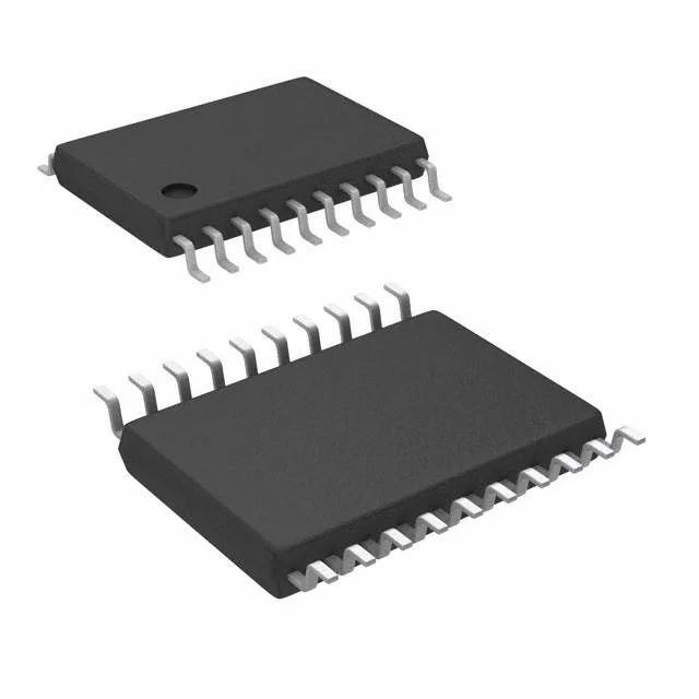
Renesas Electronics 5V41066PGGI8 — Clock & Timing ICs

Renesas 5V41066PGGI8 Clock Generator, PLL, 200MHz, 20-TSSOP

MPN5V41066PGGI8
End of Life

Renesas Electronics 5V41066PGGI8 clock generator IC, PLL-based, 200 MHz max, 1:4 fanout, HCSL/LVDS outputs, 20-TSSOP, tape and reel.

$2.16271Ref. price · indicative, final on quote
Packaging20-TSSOP (0.173", 4.40mm Width)
StockContact for availability
Lead timeIn Stock wk
MOQ1 pcs
  • 100% new & originalTraceable channels only — no refurbs, no pulls, no remarked parts.
  • Date & lot codes on quoteStated per line before you commit; label photos on request.
  • MSL-compliant ESD packingMoisture-sealed bags with indicator cards; reels photo-verified.
  • PayPal buyer protectionPay by T/T, PayPal or Payoneer — card payments covered end to end.

Specifications

5V41066PGGI8 Technical Specifications
ParameterValue
Mounting typeSurface Mount
Voltage3.135V ~ 3.465V
Frequency200MHz
Operating temperature-40°C ~ 85°C
PLLYes
InputClock, Crystal
OutputHCSL, LVDS
PackageTape & Reel (TR)
Main purposeEthernet, PCI Express (PCIe)
Case20-TSSOP (0.173\", 4.40mm Width)
Number of circuits1
Ratio - Input:Output1:4
Differential - Input:OutputNo/Yes

Product details

Clock synthesis for PCIe and Ethernet

The 5V41066PGGI8 is a PLL-based clock generator from Renesas, built to deliver low-jitter reference clocks for PCI Express and Ethernet interfaces. It accepts a clock or crystal input and produces up to four differential outputs in HCSL or LVDS format, with a maximum output frequency of 200 MHz.

What the 1:4 fanout and differential outputs mean for your design

The 1:4 input-to-output ratio means a single reference clock or crystal feeds four independent clock trees — useful for distributing a clean 100 MHz or 125 MHz reference to multiple PCIe or Ethernet PHY devices without adding separate PLLs per lane. Differential outputs (HCSL or LVDS) provide the common-mode rejection and signal integrity needed for high-speed serial links. HCSL is the standard for PCIe reference clocks; LVDS suits lower-power or longer-trace differential routing on the same part.

The 0.65 mm pitch TSSOP footprint is common in clock distribution designs, and the tape-and-reel packaging supports volume pick-and-place.

Renesas lists the 5V41066PGGI8 as Active and ROHS3 Compliant.

Frequently asked questions

What is the maximum output frequency of 5V41066PGGI8?

The maximum output frequency is 200 MHz, making it suitable for 100 MHz and 125 MHz PCIe and Ethernet reference clocks.

What output types does 5V41066PGGI8 support?

The device outputs HCSL or LVDS differential signals, selectable per application. HCSL is the standard for PCIe clocks; LVDS offers lower power for other high-speed serial links.