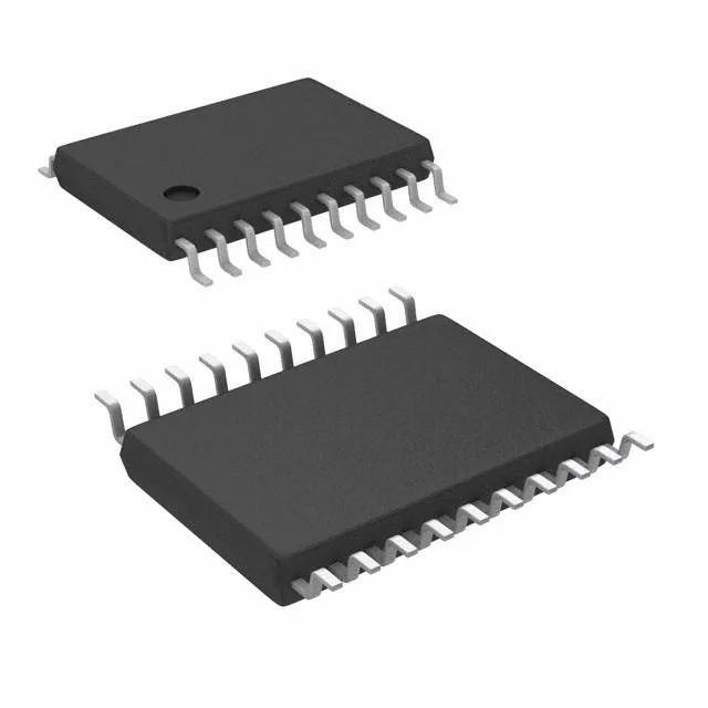
200 MHz PLL clock generator with spread spectrum — what it buys the PCIe / Ethernet clock tree
The Renesas 5V41066PGG is a single-circuit PLL clock generator aimed at Ethernet and PCI Express (PCIe) reference clock applications. It accepts a clock or crystal input and delivers up to four HCSL or LVDS outputs at frequencies up to 200 MHz, with the input side single-ended and the output side differential. The 3.135 V to 3.465 V supply range keeps it on the 3.3 V rail common in line cards and switch designs. Spread spectrum modulation is built in — that is the part's main trick for reducing EMI on high-speed serial links without adding ferrite beads or shielding cans.
1:4 fanout and differential output — routing the reference clock to multiple endpoints
The 1:4 input-to-output ratio means a single crystal or reference oscillator feeds four downstream devices — typically a PCIe root complex plus three switch/endpoint PHYs, or an Ethernet MAC plus three PHY-side SERDES blocks. Because the outputs are differential (HCSL or LVDS), the clock distribution tolerates longer board traces and noisier digital environments than a single-ended CMOS clock. The 200 MHz ceiling covers PCIe Gen1/2/3 reference clock requirements (100 MHz) with margin, and 1000BASE-T / 10GBASE-T Ethernet MAC reference frequencies. The 20-TSSOP package is a compact footprint for the fanout count; no exposed pad to route, so the layout is straightforward.
No last-time-buy window, no NRND flag.