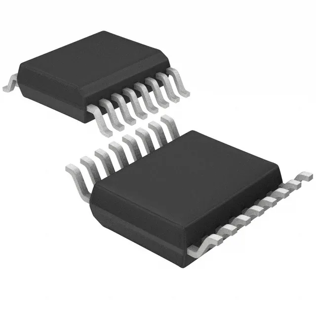
Renesas Electronics 5V41065PGG — Clock & Timing ICs

Renesas 5V41065PGG Clock Generator, PLL, 200 MHz, 16-TSSOP

MPN5V41065PGG
End of Life

Renesas 5V41065PGG clock generator IC, PLL Yes, Input Clock/Crystal, Output HCSL/LVDS, 1:2 ratio, 200 MHz max, 3.135V-3.465V supply, 0°C to 70°C, 16-TSSOP, Tube.

$3.35Ref. price · indicative, final on quote
Packaging16-TSSOP (0.173", 4.40mm Width)
StockContact for availability
MOQ1 pcs
  • 100% new & originalTraceable channels only — no refurbs, no pulls, no remarked parts.
  • Date & lot codes on quoteStated per line before you commit; label photos on request.
  • MSL-compliant ESD packingMoisture-sealed bags with indicator cards; reels photo-verified.
  • PayPal buyer protectionPay by T/T, PayPal or Payoneer — card payments covered end to end.

Specifications

5V41065PGG Technical Specifications
ParameterValue
Mounting typeSurface Mount
Voltage3.135V ~ 3.465V
Frequency200MHz
Operating temperature0°C ~ 70°C
PLLYes
InputClock, Crystal
OutputHCSL, LVDS
PackageTube
Main purposeEthernet, PCI Express (PCIe)
Case16-TSSOP (0.173\", 4.40mm Width)
Number of circuits1
Ratio - Input:Output1:2
Differential - Input:OutputNo/Yes

Product details

PLL clock generator for PCIe and Ethernet reference timing

The Renesas 5V41065PGG is a single-circuit PLL-based clock generator that accepts a crystal or single-ended clock input and delivers two differential outputs in HCSL or LVDS format. It is designed specifically for Ethernet and PCI Express (PCIe) reference clock generation, with a maximum output frequency of 200 MHz. The 1:2 input-to-output ratio means one reference source fans out to two clock lanes, which suits point-to-point links in a switch or line card where each PHY gets its own clean clock tree. Operating over the commercial temperature range of 0°C to 70°C, this part is intended for indoor, controlled-environment equipment such as network switches, routers, and server motherboards — not for industrial or outdoor deployment.

200 MHz ceiling and PCIe generation fit

The differential output (HCSL or LVDS) matches the input requirements of PCIe PHYs and Ethernet SerDes, but the single-ended input means the reference source must be clean — a crystal oscillator or a low-jitter clock module is recommended.

Lifecycle and compliance

It is ROHS3 compliant, which covers the current EU RoHS exemption list.

Package and mounting

Supplied in a 16-lead TSSOP package (4.40 mm body width) for surface-mount assembly.

Frequently asked questions

Is 5V41065PGG compatible with PCIe Gen 3 clock requirements?

No. The 200 MHz maximum output frequency limits this part to PCIe Gen 1 and Gen 2 reference clocks. PCIe Gen 3 requires a PLL rated to at least 400 MHz, such as the 9DB803DFLFT.

Does 5V41065PGG support spread spectrum modulation?

The part is described as a spread-spectrum clock generator in its title, but the evidence does not specify the modulation percentage or profile. Review the datasheet for exact spread-spectrum parameters.

What is the equivalent or replacement for 5V41065PGG?

A close functional equivalent is the 9DB803DFLFT, which also targets PCIe clocking and offers HCSL outputs, but supports 400 MHz and has a 1:8 fan-out ratio. For higher fan-out or wider temperature range, consider the 9ZXL0851EKKLF or 9ZXL1231EKILF.