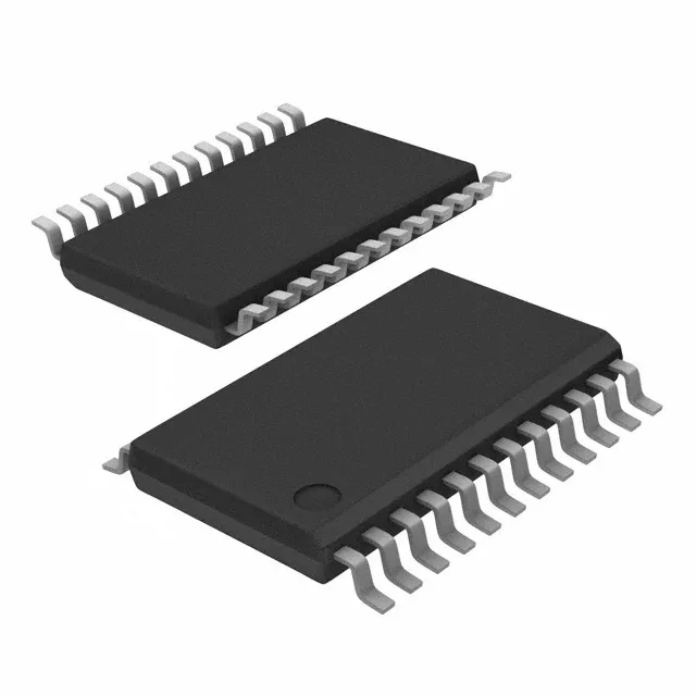
Renesas Electronics 5V2310PGGI8 — Clock & Timing ICs

5V2310PGGI8 Renesas 1:10 LVTTL Fanout Buffer 200 MHz

MPN5V2310PGGI8
End of Life

Renesas Electronics 5V2310PGGI8, Fanout Buffer (Distribution), 1:10 LVTTL input/output, 200 MHz max frequency, 2.3V to 3.6V supply, -40°C to 85°C, 24-TSSOP package

$5.28Ref. price · indicative, final on quote
Packaging24-TSSOP (0.173", 4.40mm Width)
StockContact for availability
MOQ1 pcs
  • 100% new & originalTraceable channels only — no refurbs, no pulls, no remarked parts.
  • Date & lot codes on quoteStated per line before you commit; label photos on request.
  • MSL-compliant ESD packingMoisture-sealed bags with indicator cards; reels photo-verified.
  • PayPal buyer protectionPay by T/T, PayPal or Payoneer — card payments covered end to end.

Specifications

5V2310PGGI8 Technical Specifications
ParameterValue
TypeFanout Buffer (Distribution)
Mounting typeSurface Mount
Voltage2.3V ~ 3.6V
Frequency200 MHz
Operating temperature-40°C ~ 85°C
InputLVTTL
OutputLVTTL
PackageTape & Reel (TR); Cut Tape (CT)
Case24-TSSOP (0.173\", 4.40mm Width)
Number of circuits1
Ratio - Input:Output1:10
Differential - Input:OutputNo/No

Product details

Clock fanout buffer for 200 MHz LVTTL distribution

The 5V2310PGGI8 is a 1:10 fanout buffer from Renesas, accepting a single LVTTL clock input and delivering ten LVTTL outputs with a maximum frequency of 200 MHz.

Supply voltage and input/output compatibility

Operating from a 2.3V to 3.6V supply, the buffer directly interfaces with 2.5V or 3.3V logic families without level translation. Both input and output are LVTTL, non-differential — confirmed by the Differential - Input:Output rating of No/No. This keeps the pin count low and the routing simple on a 4-layer board.

Package and footprint for PCB layout

Housed in a 24-TSSOP package (0.173" body width, 4.40 mm), the 5V2310PGGI8 uses a 0.65 mm lead pitch. The surface-mount footprint is standard for TSSOP-24, and the supplier device package is listed as 24-TSSOP. Available in Tape & Reel (TR) and Cut Tape (CT) options for both volume reflow and prototype builds.

Lifecycle and compliance status

It is ROHS3 compliant, meeting current EU directive requirements for lead-free assembly.

Frequently asked questions

What is the maximum frequency of 5V2310PGGI8?

The 5V2310PGGI8 supports a maximum frequency of 200 MHz.

Is 5V2310PGGI8 RoHS compliant?

Yes, it is ROHS3 compliant.

Does 5V2310PGGI8 have differential inputs?

No, both input and output are single-ended LVTTL (Differential - Input:Output = No/No).

When sourcing 5V2310PGGI8, what's the closest functional second-source — 5PB1104CMGK/W?

The 5PB1104CMGK/W is a clock buffer with LVCMOS I/O and a 1:4 fanout, also rated to 200 MHz, but in a smaller package and with a narrower supply range (1.71V). It is not a pin-for-pin replacement — the 5V2310PGGI8 offers a 1:10 fanout and wider supply range. Evaluate the fanout ratio and supply rails before substituting.