Renesas Electronics 5V2305NRGI — Clock & Timing ICs

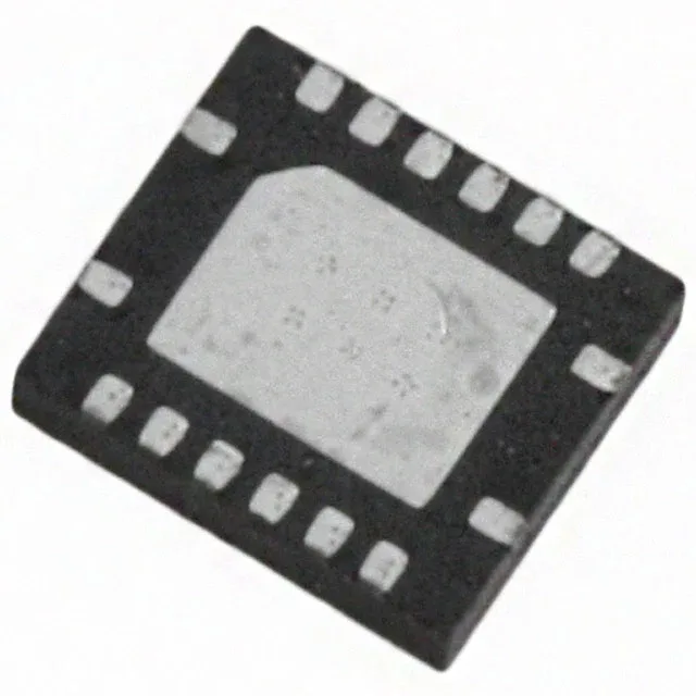
5V2305NRGI Fanout Buffer, 200 MHz, 1:5, LVCMOS, 16-VFQFPN

MPN5V2305NRGI
End of Life

Renesas 5V2305NRGI Fanout Buffer (Distribution), single LVCMOS/LVTTL input to five LVCMOS outputs, 200 MHz max, 2.3V–3.6V supply, -40°C to 85°C, 16-VFQFPN (3.5x4) exposed pad.

$3.83Ref. price · indicative, final on quote
Packaging16-VFQFN Exposed Pad
StockContact for availability
MOQ1 pcs
  • 100% new & originalTraceable channels only — no refurbs, no pulls, no remarked parts.
  • Date & lot codes on quoteStated per line before you commit; label photos on request.
  • MSL-compliant ESD packingMoisture-sealed bags with indicator cards; reels photo-verified.
  • PayPal buyer protectionPay by T/T, PayPal or Payoneer — card payments covered end to end.

Specifications

5V2305NRGI Technical Specifications
ParameterValue
TypeFanout Buffer (Distribution)
Mounting typeSurface Mount
Voltage2.3V ~ 3.6V
Frequency200 MHz
Operating temperature-40°C ~ 85°C
InputLVCMOS, LVTTL
OutputLVCMOS
PackageStrip
Case16-VFQFN Exposed Pad
Number of circuits1
Ratio - Input:Output1:5
Differential - Input:OutputNo/No

Product details

Clock fanout for single-ended rails

The Renesas 5V2305NRGI is a 1:5 fanout buffer designed to take one LVCMOS or LVTTL clock input and distribute it to five LVCMOS outputs with minimal skew. It operates from a 2.3 V to 3.6 V supply, making it a direct fit for 2.5 V and 3.3 V clock trees in industrial and communications gear. The non-differential I/O path means it handles single-ended clocks only — no CML, LVPECL, or LVDS inputs.

200 MHz ceiling — what it buys you

Rated for a maximum frequency of 200 MHz, this buffer comfortably covers the common 100–166 MHz DDR, Ethernet, and FPGA reference clock ranges. The 1:5 ratio lets a single oscillator feed five loads — typically PLLs, SerDes transceivers, or multiple ASICs — without needing a second buffer stage. At the supply tolerance end, the 2.3 V minimum ensures operation through a 3.3 V rail dipped to 2.7 V during brownout or cold-crank.

Package and thermal pad

Housed in a 16-VFQFPN with exposed pad (3.5 mm × 4.0 mm body), the part is surface-mount and requires a thermal via stitch under the pad for continuous operation near the 85 °C top end. The small footprint suits dense PCB layouts where board area is tight — typical in base stations, industrial controllers, and test equipment.

Frequently asked questions

What is the maximum operating frequency of the 5V2305NRGI?

The maximum frequency is 200 MHz, covering common 100–166 MHz clock distribution needs for DDR, Ethernet, and FPGA reference clocks.

Does the 5V2305NRGI support differential input?

No — the input is single-ended LVCMOS or LVTTL only. Differential input (CML, LVPECL, LVDS) is not supported, as confirmed by the No/No entry for differential input and output.

What is the closest functional equivalent to the 5V2305NRGI?

The 5PB1104CMGK/W is a close functional peer — same LVCMOS output type, 200 MHz ceiling, and single-ended I/O, but with a 1:4 fanout ratio instead of 1:5 and a wider temperature range (-40°C to 105°C). It runs from a 1.71 V supply, so the voltage rail differs. For a drop-in 1:5 replacement with the same supply range, no exact second-source is listed; verify pin compatibility against the datasheet.