The 200 MHz maximum frequency covers most LVCMOS clock domains for Ethernet PHYs, MCUs, and mid-speed FPGAs. The 1:8 fanout ratio lets one oscillator or PLL output feed eight loads — enough for a multi-IC board without adding a second buffer stage. Input and output are both single-ended LVCMOS; there is no differential (LVPECL/LVDS) path, so this part stays in non-differential clock trees only.
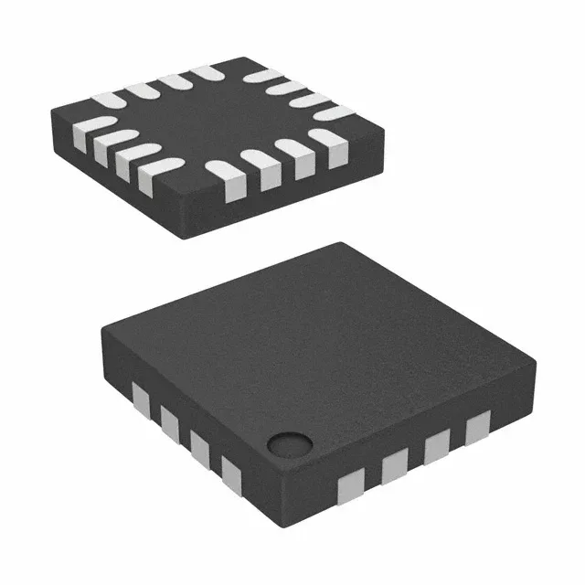
5PB1108CMGI Fanout Buffer 1:8 200MHz 16QFN
MPN5PB1108CMGI
End of Life
Renesas 5PB1108CMGI, Fanout Buffer (Distribution), 1:8 LVCMOS input/output, 200 MHz max, 1.71V~3.465V supply, -40°C to 85°C, 16-UFQFN package, Surface Mount.
$3.32Ref. price · indicative, final on quote
Packaging16-UFQFN
RoHSROHS3 Compliant
Independent supplier — new & surplus stockAuthenticity-screened · ESD-safe packingListing updated Aug 2026
Specifications
| Parameter | Value |
|---|---|
| Type | Fanout Buffer (Distribution) |
| Mounting | Surface Mount |
| Voltage | 1.71V ~ 3.465V |
| Frequency | 200 MHz |
| Operating temperature | -40°C ~ 85°C |
| Input | LVCMOS |
| Output | LVCMOS |
| Package | Strip |
| Case | 16-UFQFN |
| Number of circuits | 1 |
| Ratio - Input:Output | 1:8 |
| Differential - Input:Output | No/No |
Product details
Frequently asked questions
Will 5PB1108CMGI drop into a board designed for 5PB1104CMGK/W?
Not without a layout change. The 5PB1108CMGI is a 1:8 fanout in a 16-QFN (2.5x2.5 mm) package, while the 5PB1104CMGK/W is a 1:4 fanout in a different package. Both use LVCMOS I/O and share the same supply range, but the pinout and footprint differ.
What compliance documentation does Renesas provide for 5PB1108CMGI?
The part is ROHS3 Compliant. Renesas provides the standard RoHS certificate of compliance and material declaration datasheet. No UL or IEC certification is listed in the product record.