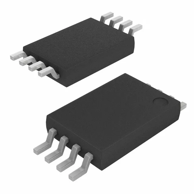
Renesas Electronics 5PB1102PGGI — Clock & Timing ICs

5PB1102PGGI Fanout Buffer, 200 MHz, LVCMOS, 8-TSSOP

MPN5PB1102PGGI
End of Life

Renesas 5PB1102PGGI, Fanout Buffer (Distribution), 1:2, LVCMOS input/output, 200 MHz max, 1.71V–3.465V supply, -40°C to 85°C, 8-TSSOP package, Tube.

$1.97Ref. price · indicative, final on quote
Packaging8-TSSOP (0.173", 4.40mm Width)
StockContact for availability
MOQ1 pcs
  • 100% new & originalTraceable channels only — no refurbs, no pulls, no remarked parts.
  • Date & lot codes on quoteStated per line before you commit; label photos on request.
  • MSL-compliant ESD packingMoisture-sealed bags with indicator cards; reels photo-verified.
  • PayPal buyer protectionPay by T/T, PayPal or Payoneer — card payments covered end to end.

Specifications

5PB1102PGGI Technical Specifications
ParameterValue
TypeFanout Buffer (Distribution)
Mounting typeSurface Mount
Voltage1.71V ~ 3.465V
Frequency200 MHz
Operating temperature-40°C ~ 85°C
InputLVCMOS
OutputLVCMOS
PackageTube
Case8-TSSOP (0.173\", 4.40mm Width)
Number of circuits1
Ratio - Input:Output1:2
Differential - Input:OutputNo/No

Product details

200 MHz LVCMOS fanout buffer for industrial clock trees

The Renesas 5PB1102PGGI is a single-channel, 1:2 fanout buffer designed to distribute LVCMOS clock signals up to 200 MHz. It accepts a single LVCMOS input and provides two identical LVCMOS outputs with minimal skew, making it a straightforward choice for splitting a reference clock to multiple loads—FPGA banks, Ethernet PHYs, or ADC sampling clocks—without adding differential conversion overhead. The supply voltage spans 1.71V to 3.465V, covering 1.8V, 2.5V, and 3.3V logic rails directly. That flexibility means the same part can serve a 1.8V core clock fanout on one board and a 3.3V peripheral clock tree on another, reducing BOM line-item count across a product family. Rated for -40°C to 85°C operation, this buffer is suited for industrial environments—outdoor telecom cabinets, factory-floor controllers, and motor-drive control boards where the ambient temperature swings well beyond commercial range.

Non-differential — what it means for your clock tree

The 5PB1102PGGI is a single-ended, non-differential buffer (No/No for differential input and output). That is the key distinction from differential fanout buffers like the 8SLVP1104ANLGI, which handles LVPECL, LVDS, or CML signals at up to 2 GHz. If your design uses differential signalling—common in high-speed SERDES or RF paths—this part will not drive those lines directly. For standard LVCMOS clock distribution at 200 MHz or below, it is a clean, low-skew fit.

Active production, no end-of-life concern

The 5PB1102PGGI carries an Active lifecycle status from Renesas. The part is ROHS3 compliant.

8-TSSOP footprint and layout notes

Housed in an 8-TSSOP package (4.40 mm width, 0.173" pitch), the 5PB1102PGGI occupies minimal board area. Surface-mount assembly is standard; no exposed thermal pad, so standard reflow profiles for TSSOP-8 apply. Place the decoupling capacitor close to the supply pin—within 2 mm—to keep the clock jitter within the datasheet limits. The 1:2 ratio means the input trace sees only one load, simplifying impedance matching.

Frequently asked questions

What is the maximum frequency of the 5PB1102PGGI?

The maximum frequency is 200 MHz, as specified for LVCMOS input and output. This is the upper limit for clean clock distribution; operate below this for best jitter margin.

Is the 5PB1102PGGI a differential clock buffer?

No. Both the input and output are single-ended LVCMOS only (differential input and output are marked No/No). For differential clock trees, consider the 8SLVP1104ANLGI or similar LVPECL/LVDS buffers.

What package does the 5PB1102PGGI come in?

It comes in an 8-TSSOP package (0.173" body width, 4.40 mm), surface-mount, supplied in Tube. The supplier device package is also 8-TSSOP.