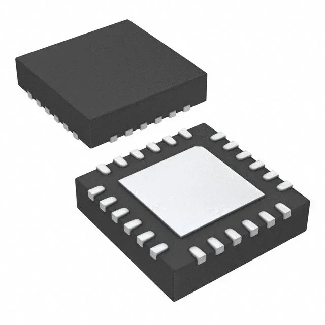
Clock tree in a 4x4 QFN
The Renesas 5P49V6965A000NLGI is a single-circuit clock generator from the VersaClock 6E family. It takes one of two differential or single-ended inputs — HCSL, LVCMOS, LVDS, LVPECL, or a crystal — and produces up to four output clocks in those same formats, all through an internal PLL with bypass capability. The maximum output frequency hits 350 MHz. The 24-QFN package (4x4 mm) with exposed pad keeps thermal impedance low in dense telecom or industrial control boards.
What the I/O flexibility means for the BOM
Because the input stage accepts HCSL, LVCMOS, LVDS, LVPECL, and crystal, and the outputs mirror that set, you avoid external level translators or AC-coupling caps on every clock line. The 2:4 input-to-output ratio means you can fan out one clean reference to four destinations — for example, one FPGA transceiver bank and three Ethernet PHYs — without adding a separate fanout buffer. The PLL bypass mode is useful when you need to pass through a clean low-jitter reference without the loop filter adding phase noise; the part still buffers and distributes it to all four outputs.
It fits outdoor telecom cabinets, factory-floor Ethernet switches, base station line cards, and test equipment that sees seasonal swings. It is not qualified to AEC-Q100, so it is not the pick for under-hood or chassis-domain automotive modules. For indoor rack-mount gear the full temperature margin is overkill, but the wide supply range and small footprint still make it a clean fit.
The VersaClock 6E family is current-production, so factory lead times apply for volume — not a surplus-only part.