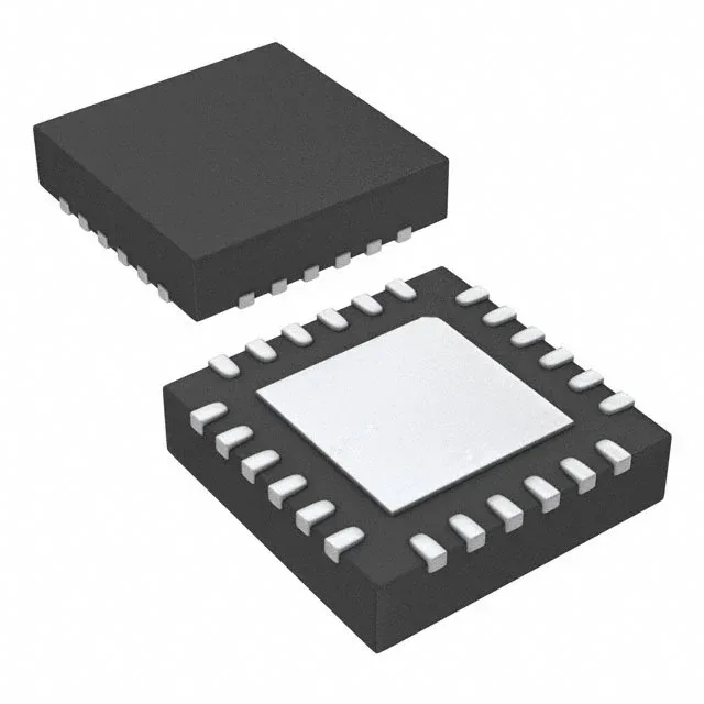
Renesas Electronics 5P49V6913A000NLGI — Clock & Timing ICs

Renesas 5P49V6913A000NLGI VersaClock 6 Clock Generator

MPN5P49V6913A000NLGI
End of Life

Renesas Electronics VersaClock® 6 Clock Generator, 5P49V6913A000NLGI, 350 MHz max, PLL with Bypass, 2:3 fanout, 24-VFQFN Exposed Pad, Tray.

$8.0Ref. price · indicative, final on quote
Packaging24-VFQFN Exposed Pad
StockContact for availability
Lead timeIn Stock wk
MOQ1 pcs
  • 100% new & originalTraceable channels only — no refurbs, no pulls, no remarked parts.
  • Date & lot codes on quoteStated per line before you commit; label photos on request.
  • MSL-compliant ESD packingMoisture-sealed bags with indicator cards; reels photo-verified.
  • PayPal buyer protectionPay by T/T, PayPal or Payoneer — card payments covered end to end.

Specifications

5P49V6913A000NLGI Technical Specifications
ParameterValue
TypeClock Generator
SeriesVersaClock® 6
Mounting typeSurface Mount
Voltage1.71V ~ 3.465V
Frequency350MHz
Operating temperature-40°C ~ 85°C
PLLYes with Bypass
InputHCSL, LVCMOS, LVDS, LVPECL, Crystal
OutputHCSL, LVCMOS, LVDS, LVPECL
PackageTray
Case24-VFQFN Exposed Pad
Divider (Multiplier)Yes/No
Number of circuits1
Ratio - Input:Output2:3
Differential - Input:OutputYes/Yes

Product details

Timing-tree fit for 350 MHz differential clocks

The 5P49V6913A000NLGI is a VersaClock® 6 clock generator from Renesas, producing up to three output clocks from two input references. Its 350 MHz maximum output frequency and differential signaling on both sides (HCSL, LVDS, LVPECL) place it squarely in high-speed serial-interface timing trees — PCIe reference clocks, 10GbE MAC/PHY, or FPGA transceiver banks that need a clean, low-jitter source.

PLL architecture and fanout planning

The internal PLL supports a bypass mode, letting you feed a clean external clock straight through when the PLL is not needed — useful for test modes or when the system clock is already clean enough. The 2:3 input-to-output ratio means two reference inputs feed three clock outputs; the third output is synthesized from one of the inputs via the PLL, so you can generate a new frequency without adding a second oscillator. All three outputs support HCSL, LVCMOS, LVDS, and LVPECL levels, so the same device can drive a PCIe reference (HCSL), a SerDes PLL (CML-equivalent via AC-coupling), and a logic-level clock (LVCMOS) from one package.

Active lifecycle and compliance posture

Renesas lists the 5P49V6913A000NLGI as Active and ROHS3 compliant.

Frequently asked questions

What is the closest functional second-source to 5P49V6913A000NLGI?

The 5P49V6965A000NLGI (VersaClock 6E) is the closest sibling — same 350 MHz max, same differential I/O, same package. The main difference is a 2:4 fanout ratio (vs 2:3 on the 5P49V6913A000NLGI), giving one extra output. If your BOM needs exactly three outputs, the 5P49V6913A000NLGI is the correct fit; if four outputs are acceptable, the 5P49V6965A000NLGI is a drop-in alternative on the same footprint and supply rails.

What compliance documentation does Renesas provide for 5P49V6913A000NLGI?

Renesas certifies the 5P49V6913A000NLGI as ROHS3 compliant. Standard documentation includes the datasheet, application notes for the VersaClock 6 family, and a material declaration sheet.