One chip, three clock functions
The Renesas 570BILFT from the ClockBlocks™ series packs three clock-management roles into an 8-pin SOIC: fanout distribution, spread-spectrum clock generation, and zero-delay buffering. A single PLL locks to an incoming clock and outputs two CMOS copies at up to 170 MHz. The 1:2 input-to-output ratio is sized for splitting a reference clock to two downstream loads — a common need on a multi-IC board where each receiver needs its own low-skew copy.
Supply rail and temperature — what to plan for
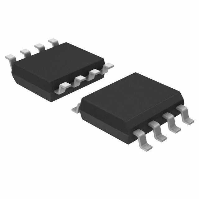
Surface-mount assembly uses an 8-SOIC package with 0.154" body width.
Active lifecycle — no end-of-life clock ticking
Input and output — no differential, all single-ended
Both input and output are single-ended — no differential pair support. If your design uses LVDS or LVPECL reference clocks, this part will not interface directly; a single-ended translator stage is needed. The input accepts a standard clock signal, and the output is CMOS, which mates directly with most MCU, FPGA, and ASIC clock inputs. The divider/multiplier is present, allowing the PLL to multiply or divide the input frequency within the 170 MHz ceiling.