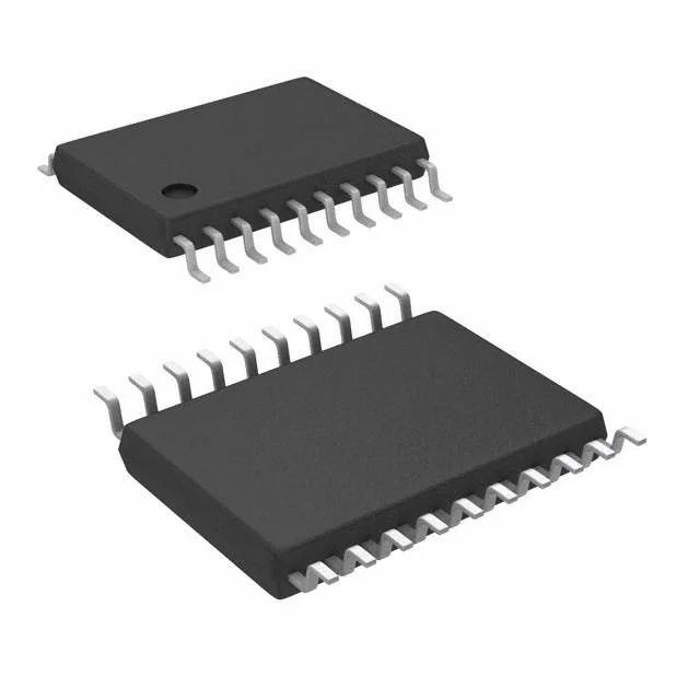
Renesas Electronics 557G-06LF — Clock & Timing ICs

557G-06LF 1:4 PCIe Clock Buffer, 200MHz, HCSL/LVDS, 20-TSSOP

MPN557G-06LF
End of Life

Renesas 557G-06LF 1:4 PCI Express clock buffer, 200MHz max frequency, HCSL/LVDS input and output, 3.3V supply, 20-TSSOP, 0°C to 70°C.

$6.08Ref. price · indicative, final on quote
Packaging20-TSSOP (0.173", 4.40mm Width)
StockContact for availability
MOQ1 pcs
  • 100% new & originalTraceable channels only — no refurbs, no pulls, no remarked parts.
  • Date & lot codes on quoteStated per line before you commit; label photos on request.
  • MSL-compliant ESD packingMoisture-sealed bags with indicator cards; reels photo-verified.
  • PayPal buyer protectionPay by T/T, PayPal or Payoneer — card payments covered end to end.

Specifications

557G-06LF Technical Specifications
ParameterValue
Mounting typeSurface Mount
Voltage3.135V ~ 3.465V
Frequency200MHz
Operating temperature0°C ~ 70°C
PLLNo
InputHCSL, LVDS
OutputHCSL, LVDS
PackageTube
Main purposePCI Express (PCIe)
Case20-TSSOP (0.173\", 4.40mm Width)
Number of circuits1
Ratio - Input:Output2:4
Differential - Input:OutputYes/Yes

Product details

PCIe clock distribution, no PLL involved

The Renesas 557G-06LF is a 1:4 fanout clock buffer designed specifically for PCI Express (PCIe) reference clock trees. It accepts either HCSL or LVDS differential inputs and delivers HCSL or LVDS outputs, with a fully differential signal path throughout — no PLL in the signal chain, so additive jitter stays low and the output phase tracks the input directly. The 2:4 input-to-output ratio lets you feed two reference clock sources (for redundancy or spread-spectrum switching) and distribute to up to four PCIe slots or endpoints.

200 MHz ceiling and what it means for your PCIe generation

Rated for a maximum frequency of 200 MHz, this buffer covers PCIe Gen1 (100 MHz) and Gen2 (100 MHz) reference clock requirements comfortably, with headroom for Gen3's 100 MHz or any 125/200 MHz non-standard clock trees. If you are planning Gen4 or Gen5 at 100 MHz, the 200 MHz ceiling still works — the buffer does not limit the data rate; the upstream clock source and the endpoint PHY set that. What matters is the additive jitter through the buffer, and the no-PLL architecture keeps it deterministic.

Supply and temperature — indoor gear only

Operates from a 3.3 V supply with ±5% tolerance (3.135 V to 3.465 V), which lines up with the standard PCIe auxiliary rail. The temperature range is commercial grade: 0°C to 70°C. That means this part is at home in servers, switches, desktop motherboards, and test equipment that lives in a climate-controlled room. Not rated for the engine bay or a rooftop enclosure in July — for that you would need the industrial-temperature sibling in the same family.

Package and footprint

Housed in a 20-pin TSSOP (4.40 mm body width), surface-mount only. The supplier device package is 20-TSSOP. Tube shipment is the standard format from Renesas; if your pick-and-place line prefers tape, the reel variant carries a different suffix. The 0.65 mm pin pitch is standard for TSSOP-20 — no surprises for the PCB layout.

Active lifecycle and sourcing posture

ROHS3 compliant (lead-free). This is a current-production part from Renesas, so no last-time-buy math or broker scavenger hunt needed.

Frequently asked questions

Can 557G-06LF be used with LVDS inputs?

Yes, the input stage accepts both HCSL and LVDS differential signals. The output can also be configured for HCSL or LVDS, making it flexible for mixed-signal clock trees.

Is 557G-06LF RoHS compliant?

Yes, it is ROHS3 compliant per the lifecycle record.

What is the equivalent or replacement for 557G-06LF?

The closest functional peer is the 9DBL411BGLFT from Renesas — also a no-PLL 1:4 PCIe clock buffer in a similar package, but its output is LP-HCSL and it runs from a 3.0 V supply. The 557G-06LF accepts a wider 3.3 V ±5% supply and supports both HCSL and LVDS I/O natively. Verify the supply voltage and output swing requirements before substituting.