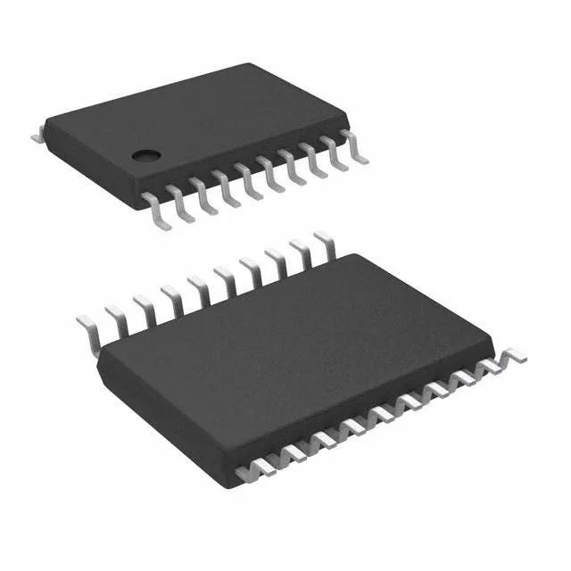
Renesas Electronics 557G-05ALF — Clock & Timing ICs

IDT 557G-05ALF PCIe Clock Generator, 200MHz, 20-TSSOP

MPN557G-05ALF
End of Life

IDT 557G-05ALF, PCI Express (PCIe) clock source IC, PLL Yes, 1:4 fanout, 200MHz max, HCSL/LVDS outputs, 3.135V-3.465V supply, 20-TSSOP, 0°C to 70°C.

$4.04Ref. price · indicative, final on quote
Packaging20-TSSOP (0.173", 4.40mm Width)
StockContact for availability
MOQ1 pcs
  • 100% new & originalTraceable channels only — no refurbs, no pulls, no remarked parts.
  • Date & lot codes on quoteStated per line before you commit; label photos on request.
  • MSL-compliant ESD packingMoisture-sealed bags with indicator cards; reels photo-verified.
  • PayPal buyer protectionPay by T/T, PayPal or Payoneer — card payments covered end to end.

Specifications

557G-05ALF Technical Specifications
ParameterValue
Mounting typeSurface Mount
Voltage3.135V ~ 3.465V
Frequency200MHz
Operating temperature0°C ~ 70°C
PLLYes
InputClock, Crystal
OutputHCSL, LVDS
PackageTube
Main purposePCI Express (PCIe)
Case20-TSSOP (0.173\", 4.40mm Width)
Number of circuits1
Ratio - Input:Output1:4
Differential - Input:OutputNo/Yes

Product details

PCIe clock source with 1:4 fanout — what it does

The Renesas (formerly IDT) 557G-05ALF is a PCI Express (PCIe) clock source IC that takes a single-ended clock or crystal input and delivers four differential HCSL or LVDS outputs at up to 200 MHz. The internal PLL cleans up the incoming reference and generates the low-jitter clock family required by PCIe root complexes, switches, and endpoints. The 1:4 fanout ratio means one input feeds four output lanes — useful for distributing a reference clock across a small PCIe switch or multiple downstream devices without adding a separate fanout buffer.

200 MHz ceiling and differential output — what they mean for the bus

The 200 MHz maximum frequency covers PCIe Gen 1 through Gen 3 reference clock requirements (100 MHz typical, with spread-spectrum modulation where needed). The differential output (HCSL or LVDS) is the standard PCIe clock signaling — the 557G-05ALF accepts a single-ended input and converts it to the differential format the PCIe PHY expects, so you don't need an external single-ended-to-differential converter. The No/Yes differential flag means the input is single-ended (clock or crystal) while all four outputs are differential.

Supply and temperature — commercial range, 3.3 V rail

The supply range is 3.135 V to 3.465 V — a tight 3.3 V ±5% window typical of PCIe clock generators. The operating temperature is 0°C to 70°C, so this part is specified for commercial/indoor equipment (servers, switches, desktop PCs, test gear) rather than industrial or outdoor environments. If the design needs -40°C operation, a different PCIe clock part with industrial temperature rating would be needed.

Package and mounting — 20-TSSOP, surface-mount

Housed in a 20-TSSOP (4.40 mm width) surface-mount package. The supplier device package is 20-TSSOP. This is a standard fine-pitch SSOP footprint — no exposed pad, so thermal dissipation is through the leads only. The shipping medium is tube, not tape-and-reel, which matters for automated pick-and-place line setup (tube-fed feeders or manual loading).

Lifecycle and compliance — active, ROHS3

The 557G-05ALF is listed as Active in production status and ROHS3 compliant.

Frequently asked questions

Is 557G-05ALF RoHS compliant?

Yes, the 557G-05ALF is ROHS3 compliant.

What is the maximum frequency of 557G-05ALF?

The maximum output frequency is 200 MHz, covering PCIe Gen 1 through Gen 3 reference clock requirements.