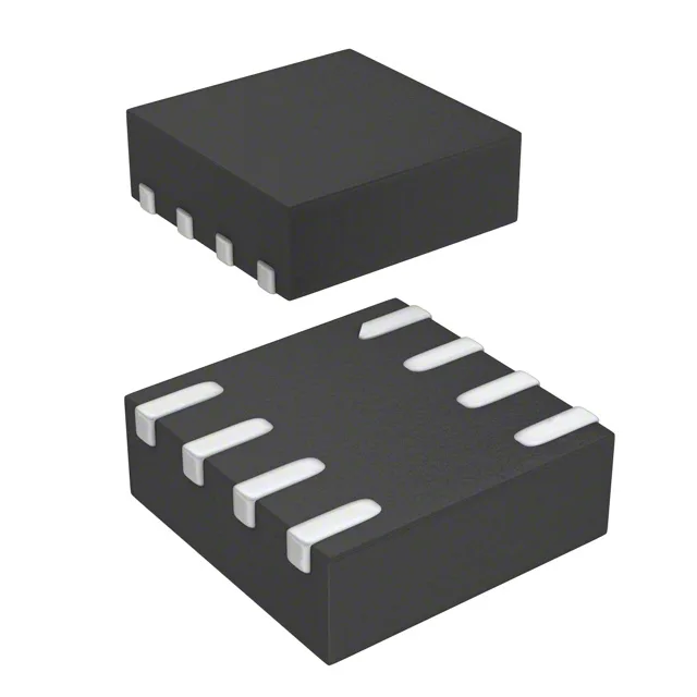
Renesas Electronics 553SCMGI — Clock & Timing ICs

553SCMGI Fanout Buffer 1:4 200 MHz 8-UFDFN

MPN553SCMGI
End of Life

Renesas 553SCMGI Fanout Buffer (Distribution), 1:4 ratio, single-ended clock input/output, 200 MHz max, 1.71 V to 3.465 V supply, -40°C to 105°C, 8-UFDFN (2x2 mm) package, surface mount.

$2.38Ref. price · indicative, final on quote
Packaging8-UFDFN
StockContact for availability
MOQ1 pcs
  • 100% new & originalTraceable channels only — no refurbs, no pulls, no remarked parts.
  • Date & lot codes on quoteStated per line before you commit; label photos on request.
  • MSL-compliant ESD packingMoisture-sealed bags with indicator cards; reels photo-verified.
  • PayPal buyer protectionPay by T/T, PayPal or Payoneer — card payments covered end to end.

Specifications

553SCMGI Technical Specifications
ParameterValue
TypeFanout Buffer (Distribution)
Mounting typeSurface Mount
Voltage1.71V ~ 3.465V
Frequency200 MHz
Operating temperature-40°C ~ 105°C
InputClock
OutputClock
PackageStrip
Case8-UFDFN
Number of circuits1
Ratio - Input:Output1:4
Differential - Input:OutputNo/No

Product details

What this 1:4 fanout buffer does on your clock tree

The Renesas 553SCMGI is a single-ended fanout buffer that takes one clock input and distributes it to four outputs, rated to 200 MHz. It is not a PLL, jitter attenuator, or format converter — it is a clean fanout element for splitting a clock signal across multiple loads while maintaining signal integrity within its bandwidth. The 1:4 ratio matches the common need for one oscillator or PLL output to feed an FPGA bank, multiple ADCs, or a set of PHY devices on the same board. Supply voltage spans 1.71 V to 3.465 V, covering common logic families from a single rail. If your clock source is differential, you need a different part or an external converter before this buffer.

Package and mounting — fits tight layouts

Housed in an 8-UFDFN package (2x2 mm body), the 553SCMGI is a small-footprint surface-mount device. The supplier device package is listed as 8-VFQFN (2x2), which is the same mechanical outline. Mounting is surface mount only — no through-hole variant exists. The small pad geometry demands careful solder-paste stencil design and reflow profile control, especially for hand-assembly or rework in a lab environment.

Temperature grade and environment

Rated for -40°C to 105°C operating temperature, this is an industrial-grade part. It is suitable for outdoor telecom cabinets, factory-floor automation controllers, and other environments where the ambient temperature can swing beyond commercial limits.

Lifecycle and sourcing posture

The 553SCMGI is listed as Active with ROHS3 compliance. There is no NRND or LTB flag on this part, so it is a safe choice for new designs and production BOMs without near-term obsolescence risk.

Frequently asked questions

What is the closest functional second-source to 553SCMGI?

The 5PB1104CMGK/W is a close functional peer — same 1:4 fanout ratio, 200 MHz max frequency, single-ended LVCMOS I/O, 1.71 V to 3.465 V supply, and -40°C to 105°C temperature range. The key difference is package: 553SCMGI comes in 8-UFDFN (2x2 mm), while 5PB1104CMGK/W is offered in Tape & Reel packaging. Verify pin compatibility and footprint before substituting.

Is 553SCMGI differential or single-ended?

The 553SCMGI is single-ended on both input and output (No/No for differential). It is not compatible with LVPECL, LVDS, or CML signal levels without an external converter.