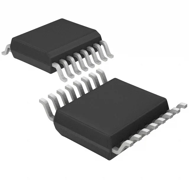
Renesas Electronics 552G-02ILNT — Clock & Timing ICs

552G-02ILNT Clock Fanout Buffer, 2:8, 200 MHz, 16-TSSOP

MPN552G-02ILNT
End of Life

ClockBlocks™ 552G-02ILNT, Fanout Buffer (Distribution), Multiplexer, 2:8 input:output, 200 MHz max, CMOS output, 2.375V-5.25V supply, -40°C to 85°C, 16-TSSOP.

$6.27Ref. price · indicative, final on quote
Packaging16-TSSOP (0.173", 4.40mm Width)
StockContact for availability
MOQ1 pcs
  • 100% new & originalTraceable channels only — no refurbs, no pulls, no remarked parts.
  • Date & lot codes on quoteStated per line before you commit; label photos on request.
  • MSL-compliant ESD packingMoisture-sealed bags with indicator cards; reels photo-verified.
  • PayPal buyer protectionPay by T/T, PayPal or Payoneer — card payments covered end to end.

Specifications

552G-02ILNT Technical Specifications
ParameterValue
TypeFanout Buffer (Distribution), Multiplexer
SeriesClockBlocks™
Mounting typeSurface Mount
Voltage2.375V ~ 5.25V
Frequency200 MHz
Operating temperature-40°C ~ 85°C
InputClock
OutputCMOS
PackageTape & Reel (TR); Cut Tape (CT)
Case16-TSSOP (0.173\", 4.40mm Width)
Number of circuits1
Ratio - Input:Output2:8
Differential - Input:OutputNo/No

Product details

What the 552G-02ILNT is and where it fits

The 552G-02ILNT from the ClockBlocks™ series is a single-circuit fanout buffer and multiplexer that takes up to two clock inputs and distributes them to eight CMOS outputs. It handles clock frequencies up to 200 MHz, making it a fit for distributing reference clocks, PCIe reference clocks, Ethernet MAC clocks, or FPGA fabric clocks across a board. The 2:8 ratio means you can select between two clock sources (primary and redundant, for example) and fan out to eight loads without adding external buffers. The supply voltage spans 2.375 V to 5.25 V. The operating temperature range of -40°C to 85°C covers industrial and most commercial environments. The 16-TSSOP package (4.40 mm width) is a surface-mount footprint common in dense mixed-signal boards. The input and output are both single-ended (No/No for differential), so this part is for CMOS-level clock trees, not differential LVPECL or LVDS distribution.

Active lifecycle — no LTB concern

There is no last-time-buy notice or NRND flag. ROHS3 compliant. For new designs and ongoing production, this part carries no imminent obsolescence risk.

Frequently asked questions

Does the 552G-02ILNT support a 3.3 V supply?

Yes, the supply voltage range is 2.375 V to 5.25 V, so 3.3 V is well within spec. The CMOS output levels at 3.3 V are compatible with 3.3 V logic families.

What is the equivalent or replacement for the 552G-02ILNT?

A close functional peer is the 5PB1104CMGK/W, which is also a clock buffer with CMOS output and 200 MHz capability, but it has a 1:4 ratio and a slightly wider temperature range (-40°C to 105°C). The 552G-02ILNT offers a 2:8 ratio, so it is not a direct pin-for-pin replacement but can serve a similar role in designs that need more fanout or input selection.