What this clock buffer does on your board
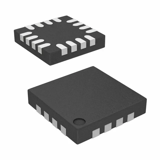
The 552-02SCMGI8 is a 2:8 LVCMOS clock buffer from Renesas, meaning it takes two input clock signals and reproduces them across eight outputs with minimal skew. The 200 MHz maximum frequency covers most FPGA reference clocks, Ethernet PHY inputs, and processor core clock trees. It accepts LVCMOS inputs and delivers LVCMOS outputs — no differential signalling, so the layout stays simple with single-ended traces. The 1.71V to 3.465V supply range lets it run on a 1.8V, 2.5V, or 3.3V rail without a separate regulator.
It ships in Tape & Reel (TR) or Cut Tape (CT) formats, surface-mount in a 16-UFQFN package (2.5x2.5 mm body).