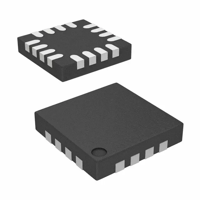
Renesas Electronics 552-02SCMGI — Clock & Timing ICs

Renesas 552-02SCMGI Clock Multiplexer, 2:8 LVCMOS, 200 MHz

MPN552-02SCMGI
End of Life

Renesas 552-02SCMGI, Type Multiplexer, Input LVCMOS, Output LVCMOS, Frequency - Max 200 MHz, Number of Circuits 1, Ratio - Input:Output 2:8, Voltage - Supply 1.71V ~ 3.465V, Operating Temperature -40°C ~ 105°C, Package / Case 16-UFQFN, Supplier Device Package 16-QFN (2.5x2.5).

$4.1Ref. price · indicative, final on quote
Packaging16-UFQFN
StockContact for availability
MOQ1 pcs
  • 100% new & originalTraceable channels only — no refurbs, no pulls, no remarked parts.
  • Date & lot codes on quoteStated per line before you commit; label photos on request.
  • MSL-compliant ESD packingMoisture-sealed bags with indicator cards; reels photo-verified.
  • PayPal buyer protectionPay by T/T, PayPal or Payoneer — card payments covered end to end.

Specifications

552-02SCMGI Technical Specifications
ParameterValue
TypeMultiplexer
Mounting typeSurface Mount
Voltage1.71V ~ 3.465V
Frequency200 MHz
Operating temperature-40°C ~ 105°C
InputLVCMOS
OutputLVCMOS
PackageStrip
Case16-UFQFN
Number of circuits1
Ratio - Input:Output2:8
Differential - Input:OutputNo/No

Product details

Clock multiplexer for redundant clock trees

The Renesas 552-02SCMGI is a 2:8 clock multiplexer that selects one of two LVCMOS input clocks and distributes it to eight LVCMOS outputs. It handles clock rates up to 200 MHz, making it a fit for FPGA reference-clock fanout, base-station timing cards, and industrial controller backplanes where a redundant oscillator or PLL source must be switched without glitching the downstream logic. The supply range spans 1.71 V to 3.465 V. The -40°C to 105°C operating range covers outdoor telecom cabinets and factory-floor enclosures where ambient temperatures climb. Packaged in a 16-QFN measuring 2.5 mm × 2.5 mm, it fits tight layout budgets on multi-layer PCBs where clock traces need short, matched routes to the fan-out targets.

What the 200 MHz ceiling means for your clock tree

The 2:8 ratio means two input clock sources (e.g., primary and backup oscillators) feed the mux, and the selected clock appears on all eight outputs. That is enough fanout for a small FPGA bank plus a few PHYs or converters without adding a separate buffer stage. LVCMOS I/O on both sides keeps the signal swing compatible with standard logic families. No level translation needed when the upstream clock source and downstream loads are both LVCMOS.

Lifecycle and compliance — no surprises

The 552-02SCMGI is listed as Active with ROHS3 compliance.

Frequently asked questions

What is the closest functional second-source for 552-02SCMGI?

The Renesas 5PB1104CMGK/W is a clock buffer with LVCMOS I/O and 200 MHz capability, but it is a 1:4 fanout buffer, not a 2:8 multiplexer. The 552-02SCMGI's 2:8 mux function is not directly second-sourced by that part. For a true 2:8 LVCMOS mux, the 552-02SCMGI is the primary choice.

Is 552-02SCMGI RoHS compliant?

Yes, it is ROHS3 Compliant, meeting the latest EU RoHS exemption limits.