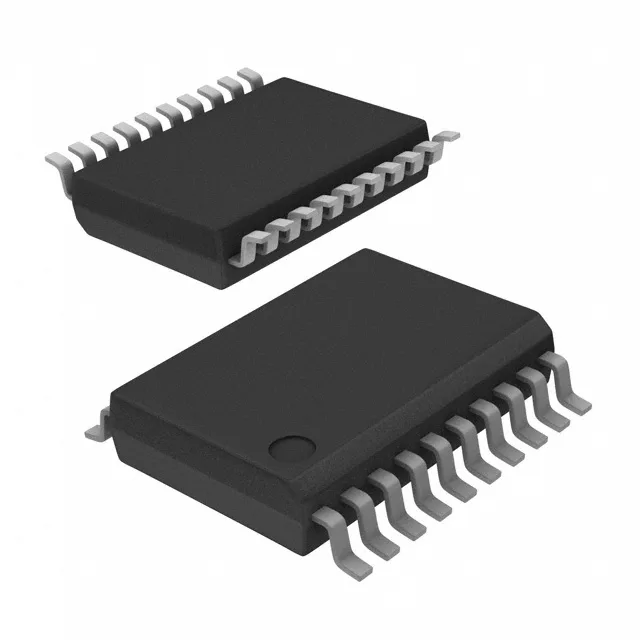
Renesas Electronics 49FCT3805DPYGI — Clock & Timing ICs

49FCT3805DPYGI Fanout Buffer (Distribution), 166 MHz

MPN49FCT3805DPYGI
End of Life

Renesas 49FCT3805DPYGI, Fanout Buffer (Distribution), 2 circuits, 1:5 ratio, 166 MHz max, CMOS/LVTTL I/O, 3V–3.6V supply, -40°C–85°C, 20-SSOP.

$3.35Ref. price · indicative, final on quote
Packaging20-SSOP (0.209", 5.30mm Width)
StockContact for availability
MOQ1 pcs
  • 100% new & originalTraceable channels only — no refurbs, no pulls, no remarked parts.
  • Date & lot codes on quoteStated per line before you commit; label photos on request.
  • MSL-compliant ESD packingMoisture-sealed bags with indicator cards; reels photo-verified.
  • PayPal buyer protectionPay by T/T, PayPal or Payoneer — card payments covered end to end.

Specifications

49FCT3805DPYGI Technical Specifications
ParameterValue
TypeFanout Buffer (Distribution)
Series49FCT
Mounting typeSurface Mount
Voltage3V ~ 3.6V
Frequency166 MHz
Operating temperature-40°C ~ 85°C
InputCMOS, LVTTL
OutputCMOS, LVTTL
PackageTube
Case20-SSOP (0.209\", 5.30mm Width)
Number of circuits2
Ratio - Input:Output1:5
Differential - Input:OutputNo/No

Product details

What this 1:5 fanout buffer does on the board

The Renesas 49FCT3805DPYGI is a non-inverting clock buffer that takes one CMOS or LVTTL input and distributes it to five outputs per bank, with two independent banks on-chip. It is a straight fanout buffer — no PLL, no jitter cleaning, no internal termination — just clean single-ended clock or signal replication rated up to 166 MHz. The 1:5 ratio per circuit means a single oscillator or clock source can feed five loads without extra external buffers, saving board area and routing complexity.

Supply and logic compatibility — 3.3 V systems

The 3 V to 3.6 V supply range maps directly onto a 3.3 V rail with margin for regulation tolerance. Input and output levels are CMOS and LVTTL, so this buffer mates cleanly with 3.3 V FPGAs, ASICs, and microcontrollers without level translation.

Temperature grade and deployment environment

Rated for -40°C to 85°C, the industrial temperature range covers outdoor telecom cabinets, factory-floor PLCs, motor drives, and base-station line cards. Not qualified for automotive under-hood (no AEC-Q100 cited), but fine for cabin or controlled industrial enclosures.

Package and footprint

Housed in a 20-SSOP (5.30 mm body width, 0.209" pitch), the package is a standard surface-mount footprint shared across many Renesas 49FCT-series clock buffers. The supplier device package is 20-SSOP; the shipping medium is Tube, not Tape & Reel — factor that into pick-and-place setup if you are running a reel-fed line.

Lifecycle and sourcing posture

The 49FCT3805DPYGI carries an Active product status with ROHS3 compliance. No NRND flag, no last-time-buy notice — it remains a current-production part. For BOM planning, this means no imminent obsolescence risk.

Frequently asked questions

Is 49FCT3805DPYGI compatible with 3.3V logic?

Yes. The supply voltage range is 3 V to 3.6 V, and both input and output are CMOS/LVTTL — it is designed for 3.3 V single-ended clock distribution.

What is the closest functional alternative to the 49FCT3805DPYGI?

The 8SLVP2108ANLGI/W is a dual-bank fanout buffer but uses differential LVPECL I/O and a 2.375 V supply — not a pin-compatible or logic-compatible substitute. For single-ended LVCMOS fanout, the 5PB1104CMGK/W is a 1:4 buffer with a 1.71 V supply and extended temperature range to 105°C, but it is a single-circuit device. Neither is a direct drop-in; the 49FCT3805DPYGI fills a specific 3.3 V, 1:5, dual-bank, non-differential niche.