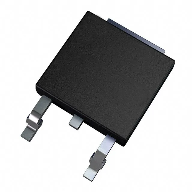
Renesas Electronics 2SJ687-ZK-E1-AY

2SJ687-ZK-E1-AY P-Channel MOSFET, 20V 20A, 7mOhm Rds(on)

MPN2SJ687-ZK-E1-AY
End of Life

Renesas 2SJ687-ZK--AY, P-Channel MOSFET, 20 V Vdss, 20 A Id, 7 mOhm Rds(on) at 4.5 Vgs, 57 nC Qg, TO-252 (DPak) surface-mount package.

$2.57Ref. price · indicative, final on quote
PackagingTO-252-3, DPak (2 Leads + Tab), SC-63
StockContact for availability
MOQ1 pcs
  • 100% new & originalTraceable channels only — no refurbs, no pulls, no remarked parts.
  • Date & lot codes on quoteStated per line before you commit; label photos on request.
  • MSL-compliant ESD packingMoisture-sealed bags with indicator cards; reels photo-verified.
  • PayPal buyer protectionPay by T/T, PayPal or Payoneer — card payments covered end to end.

Specifications

2SJ687-ZK-E1-AY Technical Specifications
ParameterValue
FET typeP-Channel
Mounting typeSurface Mount
Drain to source voltage20 V
Drive voltage (Max rds on, min rds on)2.5V, 4.5V
Current - continuous drain (Id) @ 25°C20A (Tc)
Power dissipation1W (Ta), 36W (Tc)
Operating temperature150°C (TJ)
PackageTape & Reel (TR); Cut Tape (CT)
Vgs±12V
TechnologyMOSFET (Metal Oxide)
CaseTO-252-3, DPak (2 Leads + Tab), SC-63
Rds on (Max) @ id, vgs7mOhm @ 10A, 4.5V
Gate charge (Qg) (Max) @ vgs57 nC @ 4.5 V
Input capacitance (Ciss) (Max) @ vds4400 pF @ 10 V

Product details

Low-voltage P-channel switch — 7 mOhm at 4.5 V gate drive

The 2SJ687-ZK-E1-AY: The 2SJ687-ZK--AY P-channel MOSFET has a 7 mOhm maximum on-resistance at a 4.5 V gate drive. The 57 nC gate charge at 4.5 V is moderate for a 20 A P-channel in a TO-252 package. It means the gate driver needs to source about 57 nC per switching cycle; at 100 kHz switching frequency the average gate-drive current is roughly 5.7 mA, well within the capability of a typical MOSFET driver IC.

20 V Vdss — confirm the rail voltage plus transients

The 20 V drain-source rating sets a hard ceiling. This part is sized for 5 V, 9 V, or 12 V rails where the maximum transient does not exceed 20 V. It is not a candidate for 24 V or 48 V bus switches — the margin is insufficient. The input capacitance of 4400 pF at 10 V Vds is typical for a 20 A P-channel; it does not impose unusual drive demands at moderate switching frequencies.

TO-252 package — thermal and footprint notes

The TO-252-3 (DPak) surface-mount package with a single exposed tab requires a copper island on the PCB for thermal dissipation. The datasheet specifies 1 W maximum dissipation at ambient (Ta) and 36 W at the case (Tc).

Active production — no end-of-life flags

The 2SJ687-ZK--AY carries an active product status. The part is ROHS3 compliant.

Frequently asked questions

Can 2SJ687-ZK--AY be used in high-frequency switching applications?

The 57 nC gate charge at 4.5 V and 4400 pF input capacitance at 10 V Vds are moderate values. At switching frequencies up to 100 kHz the gate-drive current requirement is about 5.7 mA average, which a standard MOSFET driver can supply. Above 200 kHz the switching losses from the gate charge and output capacitance (Coss, not listed) will dominate the dissipation budget, so the part is best suited for load-switching, OR-ing, and low-to-medium frequency DC-DC converters rather than high-frequency resonant converters.