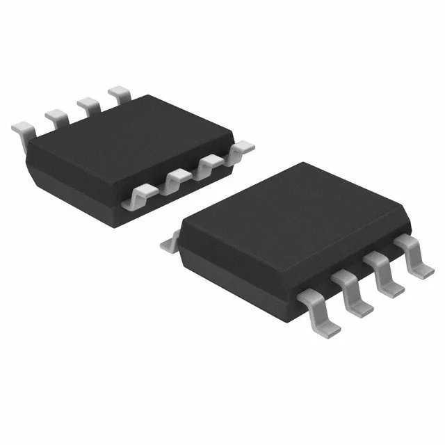
What this zero delay buffer does on your clock tree
The Renesas 2305B-1DCG is a zero delay buffer — a PLL-based clock fanout chip that takes one LVTTL input and delivers five synchronized outputs at CMOS, LVCMOS, or TTL levels. The internal PLL can be bypassed, letting the part act as a simple fanout buffer when you don't need the phase alignment. Maximum output frequency is 133 MHz, which covers most PCI, Ethernet, and general-purpose logic clock domains. The 1:5 ratio means one clock source drives up to five loads without external fanout trees or additional buffers.
Housed in an 8-pin SOIC (0.154" body width, 3.90 mm), surface-mount. Standard SOIC-8 land pattern; no surprises for the PCB layout. Ships in tube — if your pick-and-place expects tape, verify the reel option with your distributor.