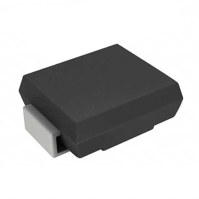
Automotive TVS diode — what the ratings mean
The 1.5SMCJ20CA-AU_R1_000A1: The AEC-Q101 qualification is the anchor for this part — it tells the sourcing engineer that the die, wafer processing, and packaging have passed the automotive stress sequence (temperature cycling, high-temperature reverse bias, power temperature cycle, and ESD characterization per AEC-Q101). For a TVS used in any chassis-domain or powertrain-adjacent circuit, that qualification level is the gate, not a nice-to-have. Without it, the part cannot enter a typical Tier-1 BOM for an OEM program. That 46.3 A figure tells you the diode is sized for short-duration industrial or automotive surge transients — IEC 61000-4-5 combo waves, load-dump peaks, and motor-inductive kick — where the clamping voltage at 46.3 A stays within 32.4 V to protect the downstream IC. Power line protection is flagged No — this part protects individual signal or control lines, not bus rails that distribute power across a harness.
Package, thermal margin, and deployment fit
The DO-214AB (SMC) package is the workhorse footprint for 1.5–3 kW TVS diodes — standard pad layout, compatible with standard pick-and-place, and widely supported across second-source manufacturers. For automotive under-hood deployments this gives 25°C of margin above the typical 125°C ambient ceiling (derating the 150°C TJ_max by the 20°C thermal resistance delta), so there is headroom for short transients — but confirm the board-level thermal resistance against your enclosure airflow before committing to a dense layout.