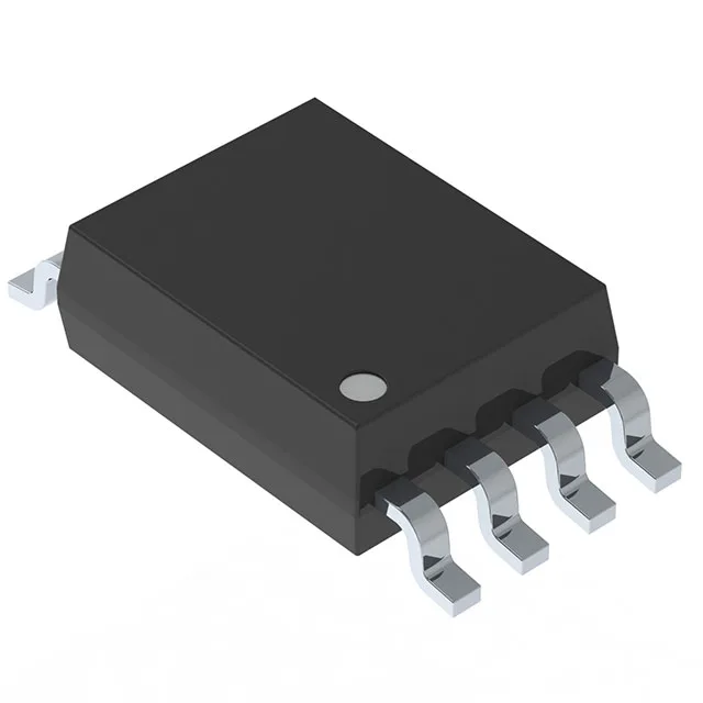
Gate-drive isolation with 5 kVrms and 100 kV/µs CMTI
The onsemi NCD57090ADWR2G is a single-channel digital isolator built for driving power-switch gates across a reinforced isolation barrier. Its 5000 Vrms isolation rating covers the creepage and clearance needed in motor drives, inverters, and industrial power supplies where the control side must stay galvanically separated from the high-voltage DC bus. The 100 kV/µs minimum common-mode transient immunity means the output state holds through the fast voltage slewing that happens when an IGBT or SiC FET switches — a 10 kV/µs edge on the bus will not glitch the gate signal.
6.5 A peak drive with matched 13 ns edges
Peak output current is 6.5 A for both source and sink, which directly charges the gate capacitance of a medium-power IGBT or SiC MOSFET in the tens-of-nC range. The 13 ns typical rise and fall times keep the Miller plateau short, reducing the dead-time margin you must budget in the switching cycle. Propagation delay is 90 ns max, symmetrical between tpLH and tpHL — this symmetry simplifies the dead-time calculation because the turn-on and turn-off delays track each other across temperature.
Capacitive coupling vs optocoupler trade-offs
The NCD57090ADWR2G uses capacitive coupling rather than an LED-and-photodiode optocoupler. Capacitive isolators typically deliver lower propagation delay, better delay matching, and higher CMTI than optocouplers in the same isolation class — the 100 kV/µs figure is well above what most optocoupler-based gate drivers achieve. The trade-off is that capacitive isolators need a clean bias supply on the output side; the 0 V to 32 V output supply range covers standard +15 V and -5 V gate drive rails.