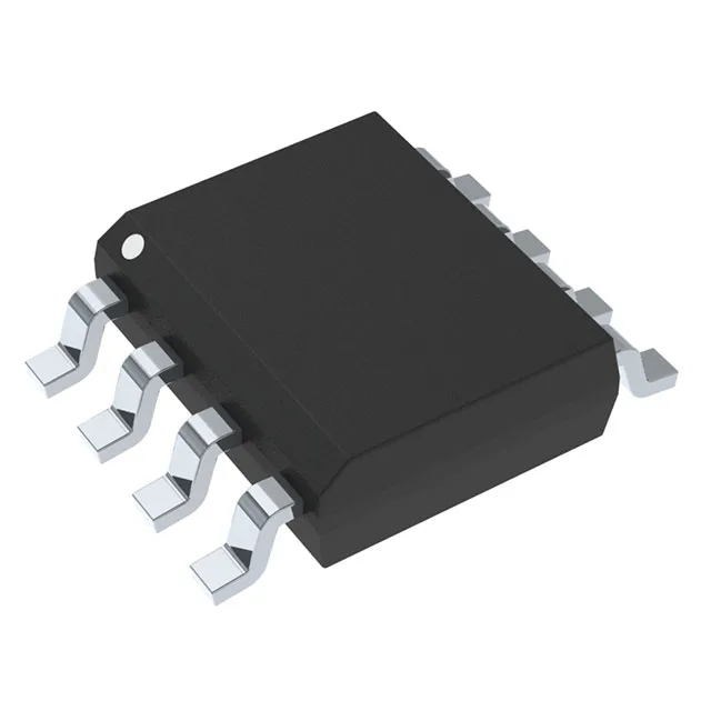
Package and board integration — 8-SOIC narrow body
The NCD57085DR2G comes in an 8-SOIC narrow-body package (3.90 mm width) with a surface-mount footprint that matches standard SOIC-8 gate driver isolator layouts. The 2500 Vrms isolation rating is specified across the package — the creepage distance between input and output sides on the 8-SOIC narrow body is approximately 4.0 mm, which meets the basic insulation requirements for 400 VAC systems per IEC 60747-17. For reinforced insulation at higher working voltages, a wider-body package or additional board-level clearance is needed.
7 A gate drive — what the peak current means for the switching loop
The 7 A peak source and sink current drives the gate charge of large IGBT modules (up to 600 A / 1200 V class) and SiC MOSFETs in a single switching event without an external booster stage. The 10 ns typical rise time into a 10 nF gate load means the Miller plateau is crossed in under 30 ns — fast enough for 100 kHz hard-switching but demanding on the gate loop inductance. The 90 ns maximum propagation delay and 25 ns maximum pulse-width distortion keep the input-to-output timing consistent across temperature and supply voltage. For a 100 kHz PWM signal with a 10 µs period, the 90 ns delay adds 0.9 % dead-time error — the controller's dead-time compensation must account for this.
100 kV/µs CMTI — why it matters for motor-drive and traction inverters
The 100 kV/µs minimum common-mode transient immunity means the isolator's output state does not glitch when the switching node voltage slews at 100 kV/µs — a typical IGBT turn-on edge in a 600 V DC bus inverter produces a dv/dt of 50–80 kV/µs at the high-side driver's ground reference. The 100 kV/µs CMTI provides margin above the worst-case inverter edge. Capacitive coupling technology inherently provides higher CMTI than optocoupler-based isolators because the coupling capacitance is smaller (typically 0.5–1 pF) and the common-mode displacement current is lower. The trade-off is a slightly higher isolation barrier capacitance, which can couple switching noise back to the input side if the layout lacks a low-impedance return path.
Automotive-grade qualification and compliance documentation
This means the part has passed the full suite of automotive reliability tests: pre-conditioning, temperature cycling, HAST, high-temperature storage, and ESD sensitivity per JEDEC JESD22. The Automotive grade is listed explicitly in the part's specification. The part is ROHS3 compliant and carries VDE approval — the VDE mark certifies compliance with IEC 60747-17 for reinforced isolation in safety-critical applications. The active lifecycle status means onsemi continues to manufacture the part with no end-of-life notice; new designs can commit to this order code without a last-time-buy risk.