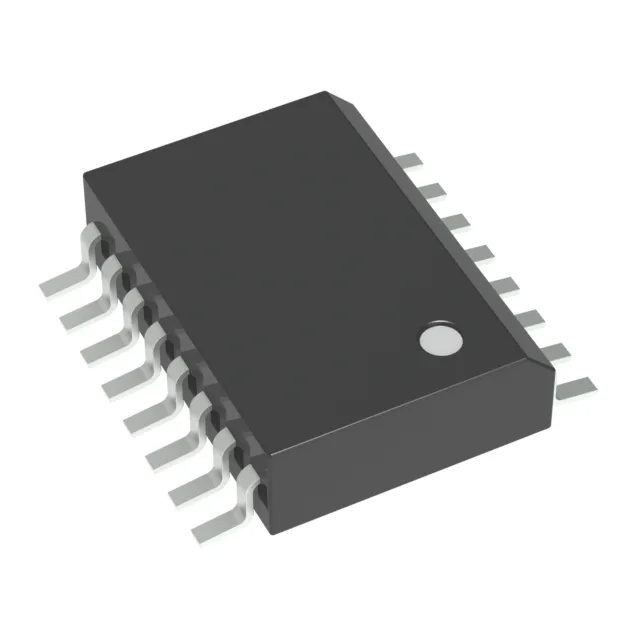
onsemi NCD57001DWR2G — Digital Isolators

onsemi NCD57001DWR2G Digital Isolator, 5000Vrms

MPNNCD57001DWR2G
End of Life

onsemi NCD57001DWR2G single-channel digital isolator, capacitive coupling, 5000Vrms isolation, 7.8A/7.1A peak output, 16-SOIC wide-body, -40°C to 125°C.

$4.99Ref. price · indicative, final on quote
Packaging16-SOIC (0.295", 7.50mm Width)
StockIn Stock (14)
Lead time3-5 Days wk
MOQ1 pcs
  • 100% new & originalTraceable channels only — no refurbs, no pulls, no remarked parts.
  • Date & lot codes on quoteStated per line before you commit; label photos on request.
  • MSL-compliant ESD packingMoisture-sealed bags with indicator cards; reels photo-verified.
  • PayPal buyer protectionPay by T/T, PayPal or Payoneer — card payments covered end to end.

Specifications

NCD57001DWR2G Technical Specifications
ParameterValue
Mounting typeSurface Mount
Voltage - isolation5000Vrms
Voltage - output supply0V ~ 24V
Current - peak output7.8A, 7.1A
Current - DC forward (If)10 mA
Operating temperature-40°C ~ 125°C (TJ)
Pulse width distortion15ns
Approval agencyUL, VDE
PackageTape & Reel (TR); Cut Tape (CT)
TechnologyCapacitive Coupling
Case16-SOIC (0.295\", 7.50mm Width)
Number of channels1
Rise (Fall time)10ns, 15ns
Propagation delay tpLH (tpHL)90ns, 90ns
Common mode transient immunity100kV/µs

Product details

Isolation and drive capability for gate-drive applications

The NCD57001DWR2G is a single-channel digital isolator from onsemi built on capacitive coupling technology, delivering 5000Vrms of galvanic isolation in a 16-SOIC wide-body package. It is designed specifically as an isolated gate driver for power switches — the 7.8A peak source and 7.1A peak sink output directly drive the gate capacitance of IGBTs and SiC MOSFETs without an external buffer stage. The 100kV/µs minimum common-mode transient immunity (CMTI) means the output stays latched to the correct state when the floating ground plane jumps through a hard-switching event — a requirement for motor-drive and inverter half-bridge topologies where the low-side switch sees the full DC-bus voltage slew.

Timing margins and temperature range

Propagation delay is matched at 90ns max for both tpLH and tpHL, with pulse-width distortion held to 15ns max. The 10ns typical rise and 15ns fall time keep the gate-drive waveform edges clean enough to avoid Miller turn-on in the power switch, provided the gate-loop inductance is kept under 20nH. The 0V to 24V output supply range matches the gate-drive rails used for standard IGBTs and SiC MOSFETs.