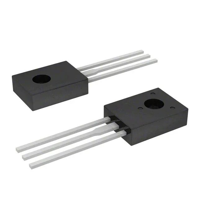
NPN power transistor — 5 A, 60 V in TO-126
The KSD1691YS is an NPN silicon power transistor from onsemi, housed in a TO-225AA / TO-126-3 through-hole package. It is rated for a continuous collector current of 5 A and a collector-emitter breakdown voltage of 60 V, placing it in the medium-current, general-purpose switching class.
Saturation voltage and conduction loss
Maximum Vce(sat) is 300 mV at 200 mA base current and 2 A collector current. At this operating point the conduction loss is 0.6 W, leaving 0.7 W of the 1.3 W total power budget for switching losses and ambient temperature derating. The 150°C maximum junction temperature sets the thermal derating curve. In a 25°C ambient with the TO-126 package mounted on a minimal heatsink, the usable continuous collector current is limited by the junction-to-ambient thermal resistance, not the 5 A silicon rating.
Active production and compliance
The through-hole TO-126-3 package is suited for manual assembly and rework environments. The collector tab is electrically common with the centre pin — board layout must account for this when heatsinking or isolating the mounting surface.