Active production — sourcing through distribution
The H11F3VM: The MOSFET output stage switches a 15 V max load with 45 µs typical turn-on and turn-off times — fast enough for most industrial logic-level isolation, but not for high-speed PWM. The 4170 Vrms isolation rating means it handles reinforced insulation in mains-referenced circuits.
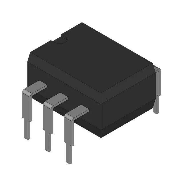
Through-hole 6-DIP — footprint and board integration
Standard 0.300-inch (7.62 mm) 6-DIP package, through-hole mounting. The 0.100-inch pin pitch mates with common DIP sockets or solders directly into a plated-through-hole PCB. Operating temperature range -40°C to 100°C covers industrial enclosures and outdoor telecom cabinets. The 1.3 V typical forward voltage at 60 mA max forward current is standard for a GaAs LED — the drive circuit needs a current-limiting resistor, not a constant-current source.
DC input, MOSFET output — what it means for the BOM
DC input type means the LED is driven by a DC forward current — no AC line coupling. The MOSFET output is a voltage-controlled switch, not a bipolar transistor, so there is no Vce(sat) drop; the on-resistance is low enough to pass analog signals up to 15 V. Single channel in a 6-pin DIP. If your BOM needs two isolated channels in one package, this is not a dual opto — you stack two H11F3VM parts or look at a multi-channel isolator. The 45 µs max switching time limits it to DC or low-frequency signal isolation, not high-speed data.