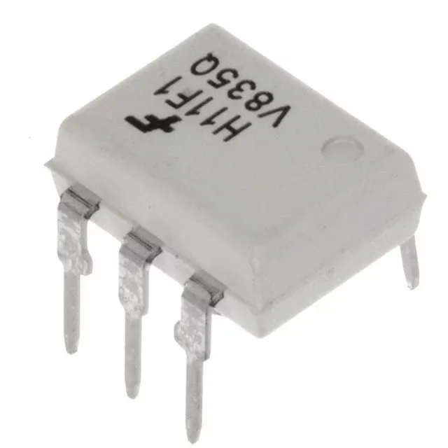
onsemi H11F1VM — Optoisolators

onsemi H11F1VM Optoisolator, 4170Vrms, Photo FET, 6-DIP

MPNH11F1VM
End of Life

onsemi H11F1VM optoisolator, photo FET output, 1-channel DC input, 4170Vrms isolation, 6-DIP (0.300", 7.62mm) through-hole package, tube.

$5.16Ref. price · indicative, final on quote
Packaging6-DIP (0.300", 7.62mm)
StockIn Stock (26)
Lead timeIn Stock wk
MOQ1 pcs
  • 100% new & originalTraceable channels only — no refurbs, no pulls, no remarked parts.
  • Date & lot codes on quoteStated per line before you commit; label photos on request.
  • MSL-compliant ESD packingMoisture-sealed bags with indicator cards; reels photo-verified.
  • PayPal buyer protectionPay by T/T, PayPal or Payoneer — card payments covered end to end.

Specifications

H11F1VM Technical Specifications
ParameterValue
Input typeDC
Output typeMOSFET
Mounting typeThrough Hole
Voltage - isolation4170Vrms
Voltage - output30V
Voltage - forward (Vf)1.3V
Current - DC forward (If)60 mA
Operating temperature-40°C ~ 100°C
PackageTube
Case6-DIP (0.300\", 7.62mm)
Number of channels1
Turn on (Turn off time)45µs, 45µs (Max)

Product details

4170Vrms isolation with MOSFET output

Rated for 4170Vrms isolation, the H11F1VM provides galvanic separation between a DC input and a MOSFET output — suited for switching low-voltage DC loads up to 30V in industrial control or instrumentation where ground loops must be broken. The photo FET output switches with typical turn-on and turn-off times of 45µs each, making it appropriate for moderate-speed signal isolation rather than high-frequency PWM.

Through-hole 6-DIP package and thermal range

Housed in a 6-DIP (0.300", 7.62mm) through-hole package, the H11F1VM mounts directly into a standard DIP socket or solders into a PCB — the 6-DIP footprint is common across many optoisolator families, easing board layout.